The requirement for digital computing machines of large storage capacity has led to the development of a storage system in which the digits are represented by a charge pattern on the screen of a C.R.T. Initial tests have been confined to commercial C.R.T.'s. Short term memory of the order of 0.2 seconds is provided by the insulating properties of the screen material. Long term memory is obtained by regenerating the charge pattern at a frequency greater than 5 cycles/second. The regeneration makes accurate stabilisation of the position of the charge pattern on the C.R.T. unnecessary.
The properties required of a storage system and its operation as part of a machine are explained with reference to a hypothetical machine. When the machine is operated in the series mode, an instruction is set up and obeyed in 600 microseconds.
1. INTRODUCTION
In order to establish a background against which the storage system described in this paper may be set, this introductory section includes a description of the system of numbers to be used in proposed computing machines, the electronic representation of this system, and a simplified diagram of a possible machine. From this diagram the properties required by a storage system are deduced.
1.1 THE BINARY SYSTEM OF NUMBERS
The problem of electronic digital computing from the engineering standpoint, lies primarily in the construction of suitable electronic devices having the same number of states, as the number of possible values of a digit, so that a one-to-one correspondence may be established between each state of the device and each value of the digit. The number of values which a digit may take depends, of course, on the system of numbers used in the machine, and it follows that it is advantageous to choose a system which can be represented electrically with ease and economy. For these reasons the binary system of numbers has become popular in recent plans for electronic digital computing machines (bibliographies 1, 2), although in the past the decimal system has been used (bibliography 3).
Systems of numbers may be derived from the common series:-
an-1bn-1 + …… + …… + a1b1 + aobo
which represents all integers with n significant figures. The decimal system, for example, is obtained if b = 10, and the a's are allowed any one of the values between, and including, 0 and 9. In the binary system b = 2 and a is either 0 or 1. The decimal number 19, say, is then 10011 in binaries, if the least significant figure is placed on the right.
The decimal, or binary, point is on the immediate right of the term aobo and the series can be continued to the right as follows:-
a-1b-1 + a-2b-2+ ……………………… + a-mb-m
1.2. ELECTRONIC REPRESENTATION OF THE BINARY SYSTEM
In the binary system only two values are possible for 'a', so that any two state electronic device may be used to represent a binary digit. Examples of such devices are a variety of flip-flop circuits, the difference in level of two D.C. or A.C. voltages, the presence or absence of a video or r.f. pulse, and the device described in this paper, namely the presence or absence of a stored charge on the inner surface of a cathode ray tube screen. As a digit is moved to different parts of the machine, its representation will change, so that at one time or another during a computation it will have adopted several of these possible forms.
If a piece of information (a number, say) is represented by k digits, the electronic quantities, corresponding with the digits, may exist either sequentially on one channel, one of k time periods being assigned to each digit, or simultaneously on k channels, one channel being assigned to each digit. The two methods of operation, which are called 'series' and 'parallel', respectively, are shown at (a) and (b) in Figure 1.1., the binary equivalent of the number 19 being used as an example. In this figure video pulses are used for digital representation, and at (a) the least significant figure is placed on the left, so that time can be shown increasing from left to right in the conventional manner.
Information may be represented 'dynamically' by pulses, which only exist transiently, or 'statically' by flip-flops, which retain the information until they are purposely reset to a standard condition. Dynamic information may be converted into static information by, for example, applying the pulses shown at (b) to five flip-flops. The set of flip-flops is called a 'staticisor'. Conversely, a circuit which converts static information into dynamic information is called a 'dynamicisor'.
A storage system could, of course, be devised using, say, the flip-flop circuit for binary representation, but the need for some new device is now shown.
1.3. THE CAPACITY OF PROPOSED STORAGE SYSTEMS
It is thought that it will be necessary to store approximately 3.2x10⁵ binary digits, in the form of 104 words, with 32 digits per word (the term 'word' is defined in Section 1.4.).
If the flip-flop circuit were used 6.4x10⁵ thermionic valves would be required, which is clearly impracticable from the points of view of the size and reliability of the equipment. Even in smaller machines the use of flip-flop circuits would defeat, to some extent, the purpose of the change from decimal to binary representation, since decimal representation by ring counters (bibliography 3), in a machine of similar capacity, would require only three times more valves; and against this would have to be set the expense of the conversion from the decimal to the binary system, and vice versa when a binary machine is used.
Recently developed two-state devices, which are far less complex than existing two- or ten-state devices, are the main justification for the change from decimal to binary representation. Further, they make digital computing machines of large storage capacity a practical proposition.
1.4. THE FUNCTION OF A STORAGE SYSTEM
The storage system is the 'memory' of a computing machine. To demonstrate this the solution of a problem will be considered and the properties required of the storage will be deduced.
The problem will be sub-divided into a sequence of simple arithmetic or logical operations externally (i.e. outside the machine), and a 'table of instructions' constructed. The instructions will be obeyed by the machine sequentially, with the proviso that at certain stages the machine may test the present state of the solution against some criterion to determine whether or not it should revert to predetermined points in the sequence. This enables the machine to carry out mathematical inductions. Each instruction in the table will require that an elementary operation be performed on, or by, a number i.e. a number will be moved from one part of the machine – a 'source', to another – a 'destination'. Every possible source and destination in the machine will be numbered, so that an instruction consists of two numbers, and can be represented as such in the binary system. The first part of the instruction, the source number 's', may for example be the 'address' of a number in the store; and the second part, the destination number 'd', may be the number allocated to one of the elementary computing circuits in the computer. Each of these elementary computing circuits corresponds with one of the arithmetical or logical operations previously mentioned. It may also be necessary to provide an instruction with a digit which determines whether an elementary computation should or should not commence immediately after a number is received by the computer, but this is omitted for simplicity. Instructions and numbers, which are collectively termed 'words', are therefore similar, the only difference between them being their function in the machine.
Since all the words applicable to a problem cannot be introduced into the machine simultaneously, they must be stored during the loading period, and, until used, during the computing period. Further, temporary storage of some type, must be provided during each elementary computing operation. In fact, for convenience, the storage may be divided into two parts, viz. the main store consisting of a number store and an instruction store, which 'remembers' words until they are required in the solution, and the temporary stores which remember numbers during the elementary computing operations.
With these preliminary observations, reference will now be made to the schematic diagram of a complete machine shown in Figure 1.2. It should be emphasised that this machine is a hypothetical one, constructed with the sole purpose of demonstrating the function of the storage system. It does, however, contain the essential framework of proposed machines.
Before computing begins, the main store will be loaded with the information relating to the problem to be solved, i.e. the instructions and numbers will be loaded into their respective stores in the order of their appearance in the solution. The conversion from written decimal to electronic binary information takes place in the unit marked 'Input'.
It is convenient in describing the operation to assume that the solution is in progress, and that the nth instruction has been obeyed. A signal will then be sent along lead 5 to the 'Control register'. The control register, which was previously registering n, the address of the nth instruction in the main store, will on receipt of the signal, register n+1. The number n+1, in binary pulse form (see Figure 1.1.(a) in a 'series' machine) will pass along lead 1 and control the 'Current instruction tree', in such manner as to cause instruction n+1 in the main store, to pass along lead 2 into the unit marked 'Current instruction'. The current instruction is the instruction which the machine is about to obey. A tree is a thermionic valve device of the staticisor type which, when controlled by k digits of an instruction, allows input or output on one only of 2k channels, the selected channel corresponding with the particular number represented by the k digits. The current instruction passes along lead 3, and is split, the source number s and destination number d controlling the s and d trees along leads 3(a) and 3(b) respectively. The number with address s in the number store can then pass along lead 4 to computing circuit d. When this elementary computation is complete, a signal is sent along lead 5 to the control register, and the cycle of events repeats. If the instruction is of a special type, the 's' and 'd' trees are controlled in such a manner as to allow the contents of computer d to pass along lead 4 into address 's' of the number store. This allows partial answers to be stored until required. A signal is then sent along lead 5 as before.
A final instruction will cause the unit marked 'Output' to operate and the converse of the input operation will occur to all or part of the number store.
The separation of the main store into number and order stores is purely artificial, and has been done to simplify the description. In practice, although the capacity of the main store is fixed, the relative capacities of the instruction and number stores will change to suit different problems.
1.5. REQUIRED PROPERTIES OF A STORAGE SYSTEM
From the previous section, it may be seen that certain properties are required of a storage system, and these are now discussed.
Sufficient attention has been given to the memory property to indicate that it is of primary importance, but in order to make practical use of a store, it must also be possible to insert, extract or erase the remembered information. The insertion of information into a store has been called 'writing'. The writing property is required by the main store during loading, and by either the main store or a temporary store during stage 4 of the operation of the machine. The stages mentioned here are numbered to correspond with activation of the similarly numbered leads in Figure 1.2.
The extraction of information from a store, 'reading' is the opposite of writing, and is required by the main store during stage 2, and output; and by either the main store or a temporary store during stage 4. Reading does not imply that the information is erased from a store, since it may be required at a later time.
'Erasing', of course, implies that information is erased from a store, but it has a second implication, namely, that a word may be written into an occupied address, deleting the word already there. This property increases the effective capacity of a store, since new information, such as partial answers, may be written over information which has been used.
To summarise, a store must have the following properties:-
(a) memory,
(b) writing,
(c) reading,
and (d) erasing.
1.6. THE PROBLEM
Briefly then the problem is to store large numbers of digits, which may be 0's or 1's, in such a way that the resulting storage system should have the properties listed above. This paper is concerned with attempts to build such a storage system, the digits being represented by charge distributions on the screen of a commercial C.R.T.
2. PHYSICAL BASIS OF THE STORAGE SYSTEM
The charge distributions corresponding with digits exist on small areas of the C.R.T. screen, and are arranged in the form of a two dimensional array. This array is produced by a television type of raster, in which the digits of a line, and the lines of the raster, are scanned sequentially. A typical display is shown in photograph 1. A 'signal' or 'pickup' plate, consisting of a sheet of metal foil, or gauze, external to the C.R.T. is closely attached to the face of the C.R.T. (see Figure 2.1.). Each area of the screen is therefore capacity coupled into a common channel, as in the iconoscope. This method of detecting changes of charge on an insulating surface has also been used to determine the secondary emission ratio of insulators using pulse technique (bibliography 4).
Having formed a general picture of the representation of digits by a two dimensional array of suitably charged areas, attention is now confined to a single small area of the screen. The potential distributions existing on this area with different types of electron bombardment, and the resulting video signals which are obtained from the pickup plate are described.
2.1. EQUIPMENT
The voltage level of the video signals is increased by connecting the pickup plate to the input of a suitable amplifier, as shown in Figure 2.1. The equivalent input circuit of the amplifier is shown in Figure 2.2.(a) where is represents the signal current due to electrons arriving at and leaving the screen surface; Cp, the capacity of the bombarded area of the screen to the pickup plate; C, the capacity of the bombarded area other than that to the pickup plate; Cs, the remaining stray capacities to earth; r, the input impedance of the amplifier; and R, the ohmic resistance due to the fact that the screen material is not a perfect insulator. The leakage time constant (Cp + C)R is known to be of the order of 0.5 seconds, while very approximate values for (Cp + C) and R are 0.005 µµf and 108 megohms respectively. The time constant Csr is less than 0.1 microsecond and r is approximately 1000 ohms. Since R>>r, the signal voltage developed across r is substantially unaffected by R, which is therefore neglected. The pickup plate current appropriate to is and flowing through Cp is very nearly (Cp/(C + Cp)) is, so that the input circuit may be reduced to that shown in Figure 2.2.(b), the final signal voltage being (Cp/(C + Cp)) ris. The amplifier, which is fully described in Section 8.1. has a bandwidth of 2 megacycles, and may be regarded as a resistance of 100 MΩ. The voltage output from the amplifier is, then, 1 volt per hundredth of a micro-amp of current flowing to, or from, the pick-up plate. There is no phase reversal in the amplifier, and current flowing from the pick-up plate gives a positive output voltage, and vice versa.
It should be noted that this equipment can only detect rates of change of surface charge on the C.R.T. screen, so that the following descriptions of potential distribution on the screen are qualitative. The absolute value of these distributions is not of primary importance to the final storage system.
2.2. POTENTIAL DISTRIBUTION WITH STEADY SINGLE SPOT
In a C.R.T. which has its deflector plates, carbon coating, and first and third anodes all connected to earth potential, and its grid, cathode and focus electrodes connected in a normal manner with respect to a negative potential (say -2000 volts), the inner surface of the screen will also be at earth potential, because it is in contact with the carbon coating. This assumes that no beam current has been present for some period of time, probably of the order of a few seconds. Now in the types of commercial C.R.T. investigated (CV1097 and CV1131), the relation between secondary emission ratio of the screen material and primary electron velocity is of the form shown in Figure 2.3. (bibliography 5). At points of operation such as A, the secondary omission ratio δo is greater than unity. This is true for all primary velocities in the range 1000 volts to 3000 volts at least. It follows that if operating under such conditions, the electron beam is switched on and falls steadily on a single spot on the C.R.T. screen, the number of secondary electrons leaving the spot and moving towards the electrode assembly, will exceed the number of primary electrons arriving at the spot. The resulting net loss of negative charge causes the potential of the bombarded spot to become positive, and its potential is then greater than that of any electrode in the tube. Later secondary electrons will therefore be ejected into a retarding electric field, and those which have emission velocities below that corresponding with the potential of the spot, will be returned to the screen. The electrons with low emission velocities will, in fact, return to the spot; those with higher velocities, repelled by other electrons, will have time to acquire an additional component of velocity parallel to the screen surface and will return to the immediate vicinity of the spot. Experiments indicate that, for times of bombardment less than 400 micro-seconds, the screen is substantially unaffected at distances greater than a spot diameter from the centre of the spot. If the effective secondary current is defined as that caused by secondary electrons which leave the spot, and are not returned to it by the retarding field, the effect of the retarding field will be to reduce the effective secondary emission ratio δ. The potential of the spot will, in fact, rise to a value Eo, thought to be about three volts, such that the retarding field causes the effective secondary emission ratio to be unity. Eo can be understood in terms of the velocity distribution of the secondary electrons (bibliography 6), indicated in Figure 2.4. (this type of distribution is known to exist in the case of metals; the distribution for insulators is not necessarily of the same type) as that point to the right of which the number of secondary electrons per unit time equals the primary current Ip. The potential of the spot will now remain constant at Eo but the longer the spot is bombarded the larger is the affected area around it. The potential distribution on the screen is summarised in Figure 2.5. in which increasing positive potential is plotted in the direction of the arrow, so that, using the analogy of gravitational field, electrons may be said to "fall" towards regions of positive potential. The depression in the distribution has been termed a "well".
The time taken to establish the potential Eo depends on the capacity per unit area of the screen, the current density of the beam, the secondary emission ratio and the velocity distribution of the secondary electrons. It follows that, with a given C.R.T., the time taken is inversely proportional to the current density. Defocussing at constant beam current, to double the spot diameter, will increase the time scale by four, whilst doubling the beam current, with constant spot size will halve the time scale. The spot capacity appears to be charged exponentially towards Eo as shown in Figure 2.6.(a), and the electron beam may be regarded as an ohmic resistance to the first order of approximation, the time constant so formed being of the order of one microsecond or less.
The net current i flowing to the spot is therefore of the form shown in Figure 2.6.(b), rising to an initial value Ip(δo - 1) corresponding with the secondary omission ratio δo, and falling approximately in an exponential manner to zero as the effective secondary emission ratio, δ, approaches unity. The area under the curve is the charge required to raise the spot capacity through Eo volts, and is therefore proportional to spot area. Since the capacity of the spot is almost entirely that to the pick-up plate, this current i will also flow from the pick-up plate to supply the required bound negative charge. The pick-up plate measures the rate of change of charge over the whole screen surface, and this means that the electrons which return to the screen around the spot will cause a slight reduction in the plate current. A further reduction, due to another effect, is now described.
2.3. EFFECT OF INTERRUPTING THE BEAM ON A SINGLE SPOT
With the spot held stationary as before, let the beam current be turned on and off by applying a square waveform of, say, 1Kc/s in frequency to the control grid of the C.R.T. When the beam is turned on for the first time, the potential distribution shown in Figure 2.5. will be established on the screen surface; but, at subsequent instants of beam turn on, substantially no change will have occurred in this distribution, because the leakage time constant of the screen (Cp + C)R is large compared with a cycle of the grid modulating waveform. It follows that only a small change in surface charge is required at these instants to maintain the potential distribution, and consequently the output voltage of the amplifier in Figure 2.1. due to this change, is negligible. However, when the beam is turned on a cloud of electrons in the secondary current, and in the beam itself, is suddenly introduced in the vicinity of the pick-up plate. This is equivalent to bringing a negative charge near to the pick-up plate and a transient current flows to the plate to supply the required induced positive charge. The electron cloud is introduced extremely rapidly if the grid modulating square wave is sharp, and the shape and time scale of the resulting amplifier output pulse, which is negative going, will be defined entirely by the transient response of the amplifier. When the beam is turned off by the square wave, the electron cloud is suddenly removed and an equal and opposite positive pulse appears at the amplifier output, as shown in Figure 2.7. The amplitude of these pulses increases with the beam current. The pulse waveforms are completely independent of spot size.
Two spots, as shown at 1 and 2 in Figure 2.8.(a), may be obtained on the C.R.T. screen by applying to a deflector plate a square waveform having half the frequency of the grid modulating waveform, and phased relative to it as shown in Figure 2.9 at (a) and (b).
If the spot is initially at 1, the potential distribution will be as previously described and is shown by the full line at (b) in Figure 2.8. The beam is now turned off, and then turned on again in position 2, causing this spot to move rapidly positive and generating the well shown chain-dotted.
If the separation between the spot centres is greater than a critical value (about 1.33 spot diameters), no other effect will occur, and at subsequent instants when the beam is turned on in the positions 1, 2, 1 and so on, this double well distribution will be maintained by insignificant changes in surface charge, making good the small leakage, as was the single well distribution described in the previous section. Consequently the amplifier output waveform will again be as shown in Figure 2.7.(b).
If, however, the separation is less than the critical value, as shown in Figure 2.8.(c), some of the secondary electrons emitted during the excavation of well 2, will be attracted to well 1 and begin to "refill" it as at (d). The extent to which well 1 is refilled depends on the separation between the spots, and the time for which well 2 is bombarded, but it is probably never completely refilled with the times of bombardment used in practice, since the fuller it gets the less likely are secondaries from well 2 to reach it. The partial refilling of well 1 causes a potential distribution in position 1 corresponding with an effective secondary emission ratio which is greater than unity, since for unity ratio a well must be excavated to the depth Eo. Therefore when the beam is turned off, moved back to position 1, and turned on again, well 1 is rapidly re-excavated to full depth, whilst well 2 is partially refilled, producing the distribution shown at (e). This process of excavating one well and partially filling the other can be repeated indefinitely, and if the system is symmetrical the charge ejected from one well will equal in magnitude that deposited in the other, since the charge ejected was deposited during the previous half cycle of operation. In fact, if the precise electrons emitted in excavating one well went immediately to the refilling of the other no signal due to changes in surface charge would be obtained. However, the excavation process is much more rapid than the refilling process, as would be expected from the fact that whereas all emitted secondaries emerge with velocities away from the well being excavated, less than half of them have a component of velocity in the direction of the well being refilled, and many of these have velocities too great to be attracted to the well, or to any part of the screen. The amplifier output pulse, at beam turn on, under these conditions will therefore be the sum of three pulses, namely, that due to excavating a partially filled well to full depth, that due to partially filling the adjacent well, and the negative pulse induced by the introduction of the electron cloud. These effects will be considered separately.
The excavation of a partially filled well to full depth establishes an additional positive charge on the screen surface, which binds an equal and opposite negative charge on the pick-up plate. This negative charge is produced by a current ie flowing from the pick-up plate into the amplifier input circuit, and a positive pulse is obtained at the amplifier output. The current ie is similar to the current i of Section 2.2., but its initial value corresponds with an effective secondary emission ratio less than δo, since the excavated well was only partially filled. This current is also slightly modified by electrons returning to the screen around the well. With a perfect amplifier the output pulse, which is indicated at (c) in Figure 2.9., would be a replica of ie.
The partial refilling of the adjacent well reduces the positive surface charge in that position, and releases an equal and opposite bound charge from the pick-up plate. Hence a current ir flows to the pick-up plate and a negative pulse is obtained at the output of the amplifier. The areas under the ie and ir waveforms are equal, because the charges involved are equal, but ir has a longer time scale and a smaller amplitude. The ir waveform is shown in Figure 2.9.(d), and its shape changes with beam current and spot size in the same manner as i or ie, (see Section 2.2.).
The induced current ic which flows because of the presence of the electron cloud has been described previously, and produces the output waveform shown again at (e).
The net output voltage of the amplifier is the sum of the three waveforms (c), (d) and (e), and is typically as shown at (f), though many variations are possible by adjusting brilliance and focus. The net pulse at the instant of beam turn on can, in fact, be made negative if the brilliance is sufficiently increased, but it is not proposed to run the C.R.T. in this condition.
2.5. SEPARATION OF DOUBLE-SPOT
It follows from the previous section, that both the amplitude and sign of the pulse obtained when the beam is turned on, with fixed beam current and focus, depend upon the separation of the spots. This pulse is the pulse marked X in Figure 2.9.(f), and its amplitude change as a function of the separation between spot centres is summarised in Figure 2.10. The pulse shown in Figure 2.9.(e) occurs about 0.2 microseconds before those shown at (c) and (d), because the current pulse in the pick-up plate, which produces the output waveform (e), is much larger and narrower than the current pulses which produce waveforms (c) and (d), and the output of the amplifier therefore responds to it with less delay time. Hence, the pulse X is never quite zero at any value of spot separation, but may be a small negative pulse followed by a small positive pulse. For this reason the positive and negative amplitudes are plotted separately. In plotting this figure only the amplitude of the pulses immediately following the instant of beam turn on is considered. The negative overshoot of the pulse X due to partially refilling the adjacent well is ignored as is the positive pulse contributed by waveform (e) when the beam is turned off.
Referring to Figure 2.10, if the separation is zero, the conditions are identical with those for a single spot and the pulse is negative, as shown in Figure 2.11.(a). The pulses in this figure are tracings taken during the experiment from the face of a C.R.T. monitoring the amplifier output. As the separation is gradually increased the negative pulse decreases in amplitude and is almost zero with a separation between centres of 0.69d, d being the diameter of the spot. During this time, the positive pulse amplitude is increasing, the waveform being as indicated at (b). The positive pulse continues to increase up to a separation d, i.e. no overlap between the spots, and then passes through a flat maximum between d and 1.16d. The pulse during this stage is shown at (c). The amplitude of the positive pulse falls off quite sharply towards zero with increased separation beyond this point, while the negative pulse amplitude increases rapidly from zero until at 1.33d the output pulse is entirely negative again as at (a). Separations greater than 1.33d, which has been called critical, give no further change.
Six curves, of which Figure 2.10. is typical, were taken for various fixed values of beam current and focus. The negative pulse, the amplitude of which gives a measure of beam current, was varied in amplitude from 16 volts to 42 volts; and the spot diameter was varied from 1mm. to 2˝mms. For all the curves, the critical separation was within the limits 1.28d to 1.38d, with the mean value 1.33d. The diameter of the spot was deduced from the amount of shift required to move the spots from coincidence to just touching. The difficulty of setting up the latter condition visually may involve errors up to about ± 5%. It has been assumed, in this section, that the diameter of a well is accurately the same as the diameter of the spot, visible on the C.R.T. screen. This must be true, with sufficient accuracy for present purposes, because the amplitude of the positive pulse will increase with separation until the two wells are touching, and it ceases to increase at the separation d (Figure 2.10).
The critical distance has, then, no absolute value. In the case of two spots of equal area, it is equal to kd, where k = 1.33 for the particular screen material investigated. (The separation experiment was performed with a CV1097 type of C.R.T.) The fact that the critical distance increases linearly with spot diameter, indicates, as might be expected, that increasing linear dimensions has no effect. For the increased separation is compensated by the increased attraction on secondary electrons by the adjacent well, due to the increased spot area.
The constant k, is determined by the screen material, and will depend on the velocity distribution of the secondary electrons, for this determines the depth Eo of a well, and therefore influences the attractive force due to the adjacent well. The secondary emission ratio, like the beam current, influences only the time taken to fill the adjacent well.
3. APPLICATION TO DIGIT STORAGE
From the phenomena described above, the following statements may be made:
(1) Either of two states of charge may be left at will at a given spot on the C.R.T. face. These states are
(a) a well of full depth, by bombarding the storage spot, ceasing the bombardment and not bombarding any other spot in the vicinity, or
(b) a partially filled well, by bombarding first a storage spot, and then another spot in the vicinity before ceasing bombardment.
(2) Charge distributions will be maintained for a time – a few tenths of a second – depending on surface leakage.
(3) Renewed bombardment (within the few tenths of a second noted under (2)) of the storage spot will give, at the instant of recommencing bombardment, a negative signal from the amplifier in case (1)(a), or a positive signal in case (1)(b).
(4) Bombardment of spots displaced by more than 1.33 spot diameters from a given spot has no influence on the potential distribution at that spot.
Item (1) above indicates a mechanism of writing a digit on a storage spot, and item (3) a mechanism of reading it. From (2) it is clear that the inherent storage time is inadequate. This can be overcome by arranging that each stored digit is read and re-written well within the inherent storage time, thus giving a new start to the stored charge with all the leakage compensated. This 'regeneration' process completely eliminates the commonly quoted objection to digit storage by charge distribution, that leakage will lead to 'spreading' and mutual interference between digits, it also has other advantages described later.
Item (4) is important in that it sets a limit to the closeness with which individual storage spots can be packed on the storage surface and hence influences the digit holding capacity of the store; this factor is discussed next.
3.1. ESTIMATED SEPARATION AND ARRANGEMENT OF STORAGE ELEMENTS
Since each storage unit of the type outlined requires a C.R.T. amplifier and regenerating mechanism, it is important economically to store as many digits as possible in each unit. It has been shown that bombardment of the screen at a distance of more than 1.33d from a storage spot has no influence on that spot. It follows that the single storage spot considered so far can be surrounded by other storage spots, provided that the separation between spot centres is greater than 1.33d. For present purposes a separation of 2d will be assumed (see Section 5.3). Furthermore, each storage spot must also have reserved an adjacent spot which can be bombarded to perform the 'filling' process.
The form and magnitude of this additional area depends on the detailed arrangement of the system, but in a simple case it may be considered as a second spot spaced d from the storage spot. The whole storage element is then contained in a rectangle d x 2d. Associated with each such element is a 'separation area' to provide clearance from other elements. The boundary of this separation area must, for safety, be at least d/2 away from the boundary of the storage element proper. The whole rectangle occupied by each digit is therefore 2d x 3d. An estimated area of 6d2 is therefore required per digit, or .06cm2 if d = 1 mm.
The screen of a c.r.t. is circular and a circular array of digits would give optimum use of the available area. This is difficult to arrange and in any case assumes complete absence of plate shadow. Accordingly a rectangular array has been chosen. A 6" c.r.t., which has an available area of 8cms x 12cms, should therefore have accommodation for 1600 digits with the estimated allocation of .06cm2 per digit. Greater numbers should become possible by improvement of focus, or by increase of C.R.T. screen area with given focus.
Bearing in mind that each digit is to be regenerated at frequent intervals, necessitating continuous scan of the whole array, the method of setting out the array is to set up the digits in a series of spaced horizontal lines as in television rasters, as mentioned earlier (see photograph (1)). With this arrangement the basic requirement is regenerative storage of a number of digits on a single horizontal line, the array being developed from the line by shifting the line perpendicular to its length through 2d after each horizontal sweep.
Many systems derived from the properties stated in Section 3, may be used to regenerate the stored information. Five such systems have been tested, and although, for reasons given later, one of these is outstanding, a brief outline is given of the alternatives. The first four of these systems operate on the pulse obtained from the amplifier when the electron beam is turned on to a spot, and all use the principle that the sign of this pulse is positive or negative depending on whether an adjacent spot within the critical distance has or has not been bombarded since the storage spot was last bombarded. The fifth system operates on a slightly different principle explained later.
3.2. SYSTEM 1 – DOT-DASH DISPLAY
Figure 3.1.(h) is a segment of a horizontal time base waveform in which short periods of constant voltage alternate with longer periods of constant rate of change. If a repetitive waveform of this kind, containing, say, 32 such segments is used to deflect a C.R.T. spot, which is intensified only during the periods of constant voltage, by applying waveform (f) to the control grid of the C.R.T., then a row of 32 dots will appear on the screen. Two of these are shown at (a).
If the separation of the dots is in excess of 1.33d each can be used independently as a storage spot, the beam being used to operate on each one in turn. The corresponding amplifier output waveform shown at (b) goes negative at the instant of beam turn on, as stated in Section 3 note 1(a), since there has been no bombardment of spots in the vicinity between bombardment of the storage spot. If the intensifying waveform is changed to (g) the dots on the C.R.T will change into short lines or 'dashes' (see (c)). The initial dots are spaced by about 3d so that the dashes may be accommodated. The amplifier output waveform is now as shown at (d). The precise nature of this waveform will be explained later, and it is necessary here only to note that the initial pulse when the beam is turned on is positive. This is in accordance with note 1 (b) of Section 3, because now there has been bombardment of spots in the vicinity of the storage spot since the storage spot was last bombarded. This bombardment took place during the previous sweep as the spot moved away from position (i) towards position (ii), (see (c)). Dots and dashes thus correspond with states 1(a) and 1(b) of Section 3 respectively and give rise to characteristic signals as defined under (3) in that section. Either dot or dash may be written in at will by using either waveform (f) or (g) of Fig.3.1. as an intensifying waveform. On a subsequent sweep dots will be 'read' as negative output pulses and dashes as positive output pulses, irrelevant parts of the amplifier output waveform being discarded by using the 'gating' waveform or strobe shown at (e).
In order to make the system regenerative it is necessary to cause dots to be re-written wherever dots are read, and dashes to be re-written wherever dashes are read. That this procedure is possible may be seen from the fact that whether a dot or a dash is to be written the intensifying waveform is the same in the time interval to to t3, whereas the amplifier output waveform has indicated which should be written well before t3, during the strobing interval t1 to t2. Hence if the intensifying signal to the C.R.T. grid is fed through a gate circuit which is controlled by the strobed amplifier output in such a way that the intensification is turned off at t3 if the control signal is negative (or zero), but is maintained until t4 if the control signal is positive, the system will be regenerative in that it will immediately re-write everything it reads. This arrangement is shown in outline in Fig. 3.4. Details of a suitable gate circuit operated by the positive control signal appear in Section 8.2.
In practice it has been found possible to replace the special time base waveform, Fig. 3.1.(h), by a simple linear time base, provided the duration ratio of waveform (g) and (f) is not less than about 2.4 to 1, and provided also that the sweep speed is such that not more than 0.7 of a spot diameter is traversed during the short intensification period of 1.9 microseconds. The dots then appear as very short lines instead of true dots.
The waveform of Fig. 3.1.(d) is of considerable interest and will now be analysed in some detail.
Let a horizontal line on the C.R.T. screen be produced by applying the waveform (a) of Figure 3.2. and its paraphased form to the X plates of the C.R.T., the grid modulating waveform being phased as at (b). Electron cloud pulses shown at (c) will of course provide a part of the amplifier output. The remainder of the output, shown at (d), is due to the following causes. When the beam is turned on initially, the positive well which is formed, is partially filled as the spot moves away from the beginning of the line. This happens in all positions previously occupied by the spot, as the spot leaves them behind, and a moving trail of positive charge is formed beneath and behind the spot as indicated in Figure 3.3.(b). When the spot reaches the end of the line, the beam is turned off, the trail of charge is left on the screen, and the potential distribution is then as indicated at (c). Now, when the beam is turned on again at the beginning of the line, a trail of charge has to be recreated, and this causes the initial positive pulse of Figure 3.2.(d). Once the trail of charge is created, there is no net change of charge on the C.R.T. screen until the remanent charge at the end of the line is approached. During this period the amplifier output is zero. As the spot approaches within the critical distance of the remanent charge low velocity secondary electrons with component velocities along the line begin to destroy the remanent charge. Since, when the beam is turned off, the potential distribution must again be as in Figure 3.3.(c), a quantity of surface charge, equal in magnitude to the created trail of charge is destroyed during this period. Hence a negative pulse, equal in area to the initial positive pulse, appears in the amplifier output voltage, as shown in Figure 3.2.(d). This negative pulse, which anticipates the cause to which it is due, namely, the turning off of the beam, has been called the 'anticipation' pulse. The net output of the amplifier is the sum of the waveforms (c) and (d) of Figure 3.2., and is shown at (e). If the length of the line is decreased waveform (e) of Figure 3.2. becomes waveform (d) of Figure 3.1. The theoretical minimum length of the line for maximum amplitude of the initial positive pulse is such that the trail of charge is completely established before secondary electrons begin to destroy the remanent charge at the end of the line. The currents flowing from and to the pick-up plate to produce the positive and anticipation pulses, respectively, are then entirely separated in time. In practice it is found that little loss in amplitude of the pulse occurs if the length of a dash is made such that the separation between centres of the initial and final spots, which form the lateral boundaries of the dash, is not less than 1.7d. With this value the positive and anticipation pulses are beginning to coalesce as shown in photograph 3(a).
By way of example, this display, and amplifier and strobed outputs appropriate to the number 19, are shown at (b), (c) and (d) in Figure 3.5. In a two state device either state may be defined as representing a '0', the other state representing a '1'. In this paper the digit will be said to be '0' when the potential distribution on the C.R.T. screen is the same as it would be if the amplifier gave zero output and the gate circuit acted appropriately.
3.3. SYSTEM 2. DASH-DOT DISPLAY
This system is identical with system 1, except that the negative pulse at beam turn on operates a gate circuit instead of the positive pulse. The positive pulse now corresponds with the digit '0' and the display is a dash as shown in Figure 3.6.(c). The negative pulse shortens the dash to a dot, and corresponds with the digit '1'. A suitable gate circuit is described in Section 8.3.
3.4. SYSTEM 3. DEFOCUS-FOCUS DISPLAY
An alternative method of achieving the choice between a positive or negative indication at beam turn on is to apply waveform (b) of Figure 3.7. to the focus electrode A2 of the C.R.T. If waveform (b) is phased relative to the grid modulating waveform as shown, the result will be a defocussed spot which suddenly becomes focussed, as shown in Figure 3.8.(a).
When the beam is turned on for the first time well 1 shown at (b) will of course be excavated by the defocussed spot. However, when the spot is focussed the shaded area at (a) will be partially filled by secondary electrons, producing the potential distribution well 2 shown at (c). At subsequent instants of beam turn on it will always be necessary to convert well 2 into well 1, and a net positive pulse will be obtained at the amplifier output. If the C.R.T. beam is turned off before it is focussed, the focussed spot will never be present, and the potential distribution is always well 1. Once this distribution is established, the output from the amplifier at beam turn on will be the negative pulse due only to the introduction of the electron cloud near to the pick-up plate. The sign of the output pulse at beam turn on is therefore positive or negative depending on whether the spot is allowed to focus or not.
If the system is operated on the positive pulse, the gate circuit of Section 3.2. is used. The only modification is to make the time base pause from t = t0 to t = t4 (Figure 3.1.). Horizontal separation of the digits is achieved by allowing the time base to run down linearly from t = t4 to t = t5, when the beam current is always off. The spot is defocussed from t = t0 to t = t3 and focussed (or blacked out) from t = t3 to t = t4.
The display appropriate to the number 19 is shown in Figure 3.6.(d).
3.5. SYSTEM 4. FOCUS-DEFOCUS DISPLAY
If the system in the previous section is operated by the negative pulse at beam turn on, in conjunction with the gate circuit of Section 3.2., the display will be as shown in Figure 3.6.(e).
Whenever the beam current is turned off, a remanent charge is left on the screen, and with a moving spot, an anticipation pulse is obtained during the next time base sweep. This gives a warning that at some later instant during the previous sweep, the beam was turned off. If the possible instants of beam turn off are predetermined by a square wave applied to a gate circuit, such as the one described in Section 8.4., and the gate circuit allows the beam to be turned off once only after an anticipation pulse has been received, then the system is regenerative. For, once established, a remanent charge will cause the beam to be turned off at the same instant of each successive sweep, and the charge will be reinstated each time. The display is indicated at (f) in Figure 3.6.
Attention will now be confined to system 1, which is summarised in Figures 3.1 to 3.5 inclusive. The remaining systems, which operate satisfactorily on a single line of digits, have been rejected; systems 3, 4 and 5, because of the difficulty of maintaining similar conditions of focus over the whole C.R.T. screen, when many lines of digits are used; and system 2 because operation on the negative amplifier output pulse is not as satisfactory as operation on the positive pulse.
Horizontal spacing between the digits on the C.R.T. screen is achieved by using the X time base waveform shown at (h) in Figure 3.1. The generation of this waveform is described in Section 8. Vertical spacing is achieved by using a television type raster. Each horizontal line contains 32 digits, i.e. a word, occupies a distance of 10cms. on the C.R.T. screen, and lasts for 256 microseconds. The blackout period is 34 microseconds. The raster has 32 lines, and at present occupies a vertical distance of 8cms. A 10cms. by 8cms. rectangle on the C.R.T. face therefore contains 1024 digits or 32 words. (photograph 1.)
The type of Y-shift generation used is intimately connected with the writing, reading and timing properties of the storage. For, not only is it necessary to scan the raster lines sequentially with the object of regenerating the stored information; but it is also essential to arrange that a word may be written into or read out of the store as soon as possible after the machine has given that instruction. A suitable circuit is now schematically described, details being deferred until Section 8.7.
4.1. Y-SHIFT GENERATOR
Figure 4.1. is a schematic diagram of a Y-shift generator. Along the top of this figure is a five-stage scale of two counter, each stage being triggered from the previous one; the first stage is triggered by the X time base blackout waveform. Each counter n is associated with a triode Tn which has a resistance R/2n-1 in its cathode lead, and the cathode of the triode is connected via a diode Dn to the grid of a pentode called the Y-shift valve (bibliography 7). The output of the Y-shift valve and its paraphased version (bibliography 7) are applied to the Y plates of the C.R.T. The circuit is completed by triodes Tn' whose cathodes are also connected to the resistances Rn. For the moment it will be assumed that the current in these triodes is cut off by negative voltages En. The outputs of the counters 1 to 5 are as shown in Figure 4.2(b) to (f), and if these are added together in the proportions 1, 2, 4, 8, 16 (i.e. 2n-1) respectively, then the resultant output is the step waveform (g). This step waveform is therefore the output of the paraphase of the Y-shift valve, since each time a triode Tn is cut off by the negative going half cycle of the waveform of counter n, a current proportional to 2n-1/R flows in R'. R' is chosen to give suitable Y-shift.
It follows from the above discussion that if the grids of the triodes Tn have negative voltages applied to them, which are sufficient to cut off the valve currents, then the line of the raster scanned by the time base can be chosen at will, by applying suitable voltages En to the triodes Tn'. For En can be chosen so that Dn either does or does not conduct (25 possibilities), and if Dn conducts a contribution 2n-1 is made to the line number. If for example with the convention that the first line in the raster is called line 0, it is desired to scan line 21, then E2 and E4 are made positive and E1, E3 and E5 are made negative. Only the diodes D1, D3 and D5 conduct and a Y-shift of 21 (20 + 22 + 24) units is produced. It will be observed that the line chosen by operating the triodes Tn' and the corresponding line of the raster produced by the triodes Tn are accurately the same, since they both depend on the resistances R/2n-1 and not on the triodes involved.
The requirement for prompt execution of an instruction by reading or writing leads to the division of the raster operation into two phases, the 'scan' and 'action' phases, controlled by waveforms applied to the grids of the triodes Tn and Tn' respectively.
During the scan phase, the raster lines are scanned sequentially with the sole object of regenerating the stored information. The remainder of the machine outside the store will not be idle during the scan phase, for, in general during this time, the next line of the store to be operative will be selected, by an instruction which controls one of the store trees. This statement is clarified by reference to Figure 4.3(a) with the schematic diagram of the complete machine in mind (Figure 1.2.). The scan and action phases are indicated in Figure 4.3(a) by the square wave. During the first scan phase shown here the control register sets up the current instruction tree (stage 1 of Figure 1.2), to the binary number n + 1. During the first action phase line n + 1 of the store is read, and instruction n + 1 passes to the current instruction unit (stage 2). The current instruction controls the s and d trees during the second scan phase (stage 3). The number in line s of the store is read and passed to destination d in the computer – or vice versa – during the second action phase (stage 4). If the computation is now complete the cycle is recommenced (stage 5). If the computation is not complete then stage 5 is prohibited until the first scan period after completion.
If the Y-shift waveform is to comply with such a programme it will be of the form shown in Figure 4.3(b), providing sequential scanning of the raster lines l, l + 1, l + 2 and so on, interspersed by the required action lines n + 1 and s. As an experimental approximation to this waveform the action line is selected by five switches, each having two positions, rather that by a 5 digit instruction in binary pulse form.
The modifications necessary to make the circuit of Figure 4.1 conform to these requirements are shown in Figure 4.4. Here the blackout waveform triggers a halver circuit, which in turn triggers the five stage scale of two counter, the waveforms involved being as shown in Figure 4.5 (a) to (g). The halver circuit is itself a scale of two counter. The halver waveform is added to each of the counter waveforms, and the resulting waveforms (h) to (l) are applied to the grids of the triodes Tn, after being D.C. restored to earth potential. In other words, the greatest voltage achieved by any of the waveforms (h) to (l) is zero volts. Further, the waveforms have sufficient amplitude to prevent current flowing in the triodes Tn except during those half cycles of the halver waveform during which they are at zero volts. Now if it is assumed for the moment that the potentials en applied to the triodes Tn' are sufficiently negative to prevent current flowing in Tn', it will be seen that during the first scan period (Figure 4.5), current flows in all the triodes Tn, so that the diodes Dn do not conduct, the Y-shift is zero and the electron beam of the C.R.T. scans line 0. But during the first action period no current flows in any Tn, so all Dn conduct, the Y-shift is at its maximum value and line 31 is selected. During the second scan period only D1 conducts, so that unit shift occurs and line 1 is scanned. But during the following action period all the diodes Dn conduct again, so that line 31 is again selected. It will be clear from such considerations that the whole raster of 32 lines will be scanned sequentially, line 31 being the action line between scans of adjacent lines. The Y-shift waveform will be as shown at 'n' except that here line 10 is being selected. In order to select line 10, say, appropriate positive (Tn' conducting) and negative (Tn' non-conducting) voltages, en, should be applied to the grids of Tn' during the action periods only, since these voltages must not interfere with the scan, i.e. with the voltages applied to the grids of Tn. To select line 10 requires a shift of 10 units during the action periods only, so that during those periods e1, e3 and e5 must be positive and e2 and e4 negative. Hence if the waveform shown at m(i) is used for e1, e3 and e5 and that at m(ii) for e2 and e4 line 10 will be selected. Here the opposite phase of the halver to the one previously considered is used and is arranged alternately to turn on and cut off current in Tn' at m(i), or is biassed well beyond cut off at m(ii). One cycle of the shift waveform under these conditions is shown at (n).
In order to change the action line, the D.C. levels of the waveforms en must be changed from 0 volts to beyond cut off of Tn' or vice versa. These voltages must not be changed during an action period, because if they are, a diagonal line will be traced across the screen by the electron beam, and stored information will be wiped out. They may, however, be changed at any time during a scan period, since they only effect Tn' which plays no part in the operation during a scan period. It is convenient to arrange that a change in voltage can only occur at the beginning of the scan period immediately following the throw of a switch. To achieve this, either the positive or the negative pips shown at (o) in the figure, which only occur at the beginning of scan periods, are applied to the input grids of five flip-flops, by means of five switches. This arrangement is shown at the bottom of Figure 4.4. When a switch is thrown, the corresponding flip-flop cannot change its state until it receives a pip. This ensures that change of state can never occur during an action period. The positive or negative voltages produced by the flip-flops are added to the halver waveform by anode followers (bibliography 7) to produce the waveforms at (m).
To summarise, the circuit causes a scan of a 32 line raster to be performed, and the action line of the raster can be selected by a suitable choice of the positions of five switches. In the final machine these switches will be replaced by five leads via which either a positive or a zero pulse may be fed to the flip-flops. If a familiar case is considered, in which the instruction is to read line 19, positive pulses (1's) will be sent to flip-flops 1, 2, and 5 only. At the beginning of each scan period, all the flip-flops will be set into a standard condition by the negative pulses shown at (o) in Figure 4.5. The five flip-flops form a staticisor. It should be noted at this point that, although the Y raster generator, X time base generator, and the circuits generating such waveforms as the strobe for the amplifier output, are essential to the operation of a single storage unit, these circuits are common to all further units. It is only necessary to repeat the C.R.T., amplifier and gate circuit, since all the C.R.T.'s and gate circuits are operated in parallel, as explained in Section 6. For this reason, a C.R.T. and its associated amplifier and gate circuit will be called a 'storage unit'.
4.2. EXPERIMENTAL INPUT
Information will eventually be introduced into the store via the input unit of Figure 1.2., which may take many forms. An experimental method of input, far too laborious to be used in practice and designed with the sole object of testing the storage unit, is as follows.
The beam is turned on 32 times during one X time base sweep, and with an empty store a negative pulse is obtained from the amplifier each time, the display being 32 lines of 32 dots. If a positive pulse is inserted into the gate circuit, in such a manner as to give the same effect as a positive pulse output from the amplifier (see typewriter input in Figure 8.2), and timed coincident with one of the instants of beam turn on, then a dash appears at the corresponding point of the display and a '1' is inserted into the store. If, further, the pulse is generated during action phases only then the dash will appear only on the action line. The circuit supplying the pulses is arranged in such a manner that pressing one of 32 keys, arranged in the form of a typewriter, causes a pulse to be generated at the corresponding beam turn on instant. A '1' is inserted in position k of line l, by operating the switches controlling the Y-shift staticisor so that line l is the action line, and then pressing key k of the typewriter. Once inserted the digit (k,l) is regenerated, and remembered by the store indefinitely.
A '1' may be erased from the store by interrupting the regenerative loop during the time that the '1' would normally be regenerated. This is conveniently done by switching the action line into the appropriate position, inverting the positive pulse from the typewriter, and applying the resulting negative pulse to the suppressor grid of V1 in the gate circuit (see Figure 8.2.). Thus, although the control grid of this valve is turned on by the positive pulse from the amplifier appropriate to a dash, no anode current will flow in the valve, and the display will be converted into a dot.
It follows that the typewriter unit may either insert or erase a '1', and that a single pole, double-throw switch may be used to select either of these alternatives.
If the input to the gate circuit from the amplifier is connected to earth potential for a period longer than a raster period, then the store will be filled (dashes everywhere), for the control grid of V1 will be turned on during every strobe period. If, on the other hand, the output of the amplifier is disconnected from the gate circuit for a period longer than a raster period, the store will be emptied.
5. FACTORS INFLUENCING OPERATING CONDITIONS
It is now possible to fill or empty the store, and, by means of three control systems, namely, the insert-erase switch, the typewriter and the Y-shift staticisor, to change the state of digit (k,l). Specific patterns, such as the one shown in photograph 1, may therefore be written into the store, in order to test the memory of the storage unit. The pickup plate prevents direct photography, and a monitor C.R.T. wired in parallel with the storage C.R.T. was photographed. During the initial tests many memory periods of between one and two hours were recorded.
By adding a sixth unit to the Y-shift generator a 64 line raster was produced, and the storage capacity doubled (2048 digits). The pattern shown in photograph 2 was then written into the store, and was remembered for four hours before the equipment was switched off. It is interesting to note that in this time approximately 7.5 x 10⁸ opportunities occurred for a change in the pattern to take place, due to possible spurious pulses occuring during strobe periods.
The factors influencing the operating conditions used to obtain these results will now be described. It will be seen that a compromise has been made between conflicting factors.
5.1. PRIMARY ELECTRON VELOCITY
From Section 2 it follows that the third anode voltage of the C.R.T. should be such that the primary electron velocity corresponds with a screen secondary emission ratio greater than unity. With the screens used in commercial C.R.T.'s a further limitation is imposed, and this is now discussed.
The signal output from the amplifier normally produced by scanning a line on the C.R.T. screen is shown in Figure 3.2.(e). However, if the line is moved to some positions on the screen the output is as shown in Figure 5.1. Disturbances of the type shown at X are thought to be caused by the following imperfections in the screen. Firstly, the screen may contain small particles of carbon, which have a secondary emission ratio less than unity for all primary electron velocities. When such particles are subjected to electron bombardment they will receive more electrons from the primary beam than they lose by secondary emission. The particle will therefore accumulate negative charge, and it will continue to do so until its potential is approximately cathode potential. Secondly, as can be seen by the naked eye, the screen material is perforated at several points. The operative screen material at these points is glass, which, as indicated in Figure 5.2., has a much lower inversion point B (about 1000 volts) than that of the true screen material. At operating voltages above that corresponding with the point B, the glass will therefore have a secondary emission ratio less than unity. The very small areas of glass uncovered by the perforations of the screen material will therefore, under electron bombardment, accumulate electrons until they are reduced to the potential corresponding with the point B.
In either of the above cases, small regions of the screen under electron bombardment will be at potentials which are very negative with respect to the remainder of the screen if a high accelerating voltage is used. Now the operation of the storage system is based on the fact that the potential distribution formed at a region P depends on whether an adjacent region within the critical distance has, or has not, been bombarded, since P was last bombarded. If such an adjacent region has been bombarded, the potential distribution at P is changed by secondary electrons arriving at P from the bombarded point. If, however, a screen imperfection exists between P and the adjacent region, some of the secondary electrons will be prevented from reaching P by the potential barrier produced by the imperfection. P will, in fact, always tend to operate as a point which has not had bombardment in its vicinity. In the dot-dash system the effect is, therefore, that if the imperfection occupies an area of the screen sufficiently large when compared with the spot area, than it is impossible to write a '1' into the store at P.
The screen imperfection signal X in Figure 5.1. consists of an anticipation pulse followed immediately by the positive pulse due to re-establishing the trail of charge (see Section 3.2.). This will be understood if it is remembered that, as the spot passes through the imperfection, some of the secondary electrons, which would normally return to the part of the screen behind the spot, are prohibited from doing so by the created potential barrier. A remanent charge must therefore exist in front of the imperfection and this produces an anticipation pulse during the following scan. The trail of charge is partially destroyed when the anticipation pulse is created, but it is reformed when the imperfection has been passed by the spot and this reformation produces the positive pulse. It is found that if the ratio of the peak to peak amplitude of the screen imperfection signal to the amplitude of the positive signal obtained when the beam is turned on (see W in Figure 5.1.), is plotted as a function of the accelerating voltage applied to the primary electrons, then the result is as shown in Figure 5.3. (bibliography 8). As might be expected from the previous discussion, the imperfection signals due to glass (or impurities with a similar inversion point) vanish when the accelerating voltage is reduced to the value corresponding with the point B in Figure 5.2., because at this voltage there is no potential barrier. The amplitude of the signals due to carbon decreases linearly as the accelerating voltage is decreased, and tends to zero as the accelerating voltage approaches zero. These results were obtained with a CV1131 type of C.R.T., which had a soft glass envelope, and the particular imperfection signals plotted were the largest which occurred at any point of the screen. No C.R.T. has yet been found with more than one carbon imperfection. The number of glass imperfections with ratios greater than 0.1 (but less than 0.2) is about twenty at 1,400 volts.
With these results in mind it was decided to operate the storage C.R.T. at 1,400 volts. The C.R.T. was not specially selected, except that it had a hard glass (inversion point approximately at 1200 volts) envelope, and there was a carbon imperfection in the screen. This C.R.T., which stored the information for photographs 1 and 2, has been used for a period of three months, and no difficulties have arisen due to screen imperfections.
5.2. STORAGE CAPACITY OF A SINGLE C.R.T.
The storage capacity of a single C.R.T. is determined primarily by the accuracy of focus, and its uniformity over the used area of the C.R.T. screen. For maximum capacity, the C.R.T. should therefore be operated at the highest possible accelerating voltage. With present screens, the imperfections limit this voltage to 1,400, and it is apparent that an attempt should be made to produce a more perfect screen, with the consequent increase in storage capacity. This is being attempted.
Although, for constant beam current, the amplitude of the positive signals obtained when the beam is turned on will decrease as the focus is improved, no difficulty is anticipated, because, as shown in photograph 3, excellent signal/noise ratio is obtained with the present spot size (about 1 mm. diameter). Loss of signal current may therefore be compensated by increased amplifier gain.
As shown in photograph 2, 2,048 digits have been stored, the area occupied on the storage tube being 154 sq. cms. (11cms. x 14cms.). In photograph 1, the area occupied by 1,024 digits is 64 sq. cms. (10cms. x 6.4cms.). The deterioration in the uniformity of focus over the larger area can be seen by the fact that for satisfactory operation – negligible interference between digit areas – the area occupied by 2,048 digits is more than twice that occupied by 1,024 digits.
5.3. ACTION LINE LIMITATION OF STORAGE CAPACITY
The conception of critical distance between two adjacent spots cannot be applied, without reservation, to determine the separation required between any two charged areas of a raster for negligible mutual interference. For the net electric field at a spot under electron bombardment is no longer due to a single adjacent charged area, but to all the remaining charged areas of the raster. It follows that the required separation is greater than the critical distance previously defined, and this is particularly true for the areas comprising the edges of the raster, where the net lateral electric fields are greatest.
The method adopted to determine the required separation experimentally is to adjust the focus, and separation between areas, until the relevant positive signals obtained at any point of the raster, are not decreased by more than 5% by mutual interference. It is found to be sufficient to examine only those areas in the corners and centre of the raster.
Since a small amount of mutual interference between adjacent charged areas is allowed to occur, the time of bombardment of the areas becomes important, particularly when this time is only of the order of 1 microsecond. (The time of bombardment of the areas is determined by the velocity with which the spot travels across the C.R.T. screen. This velocity is discussed in the next section.) From Figure 2.11. it can be seen that in the double spot experiment bombardment times less than 2 microseconds would produce little filling of the adjacent well. If, then, some areas of the raster are scanned more frequently than others, more mutual interference will occur in these regions. This will happen when the store is part of a computing machine and it is necessary to read or write into the store frequently during one raster period, for under these circumstances certain lines of the raster will be scanned more often than other lines. With a 32 line raster, and the method of raster generation described in Section 4, it is never possible to scan a particular line more than 33 times as often as the adjacent lines. For in one raster period this line would be scanned once during a scan period, and 32 times during action periods at most.
To determine the extra degree of separation between digit areas required to nullify this effect, the following procedure was adopted. It was arranged for the C.R.T. to be normally blacked out by halver waveform during action periods. A circuit triggered by the waveform of the last counter in the Y-shift generator, and re-triggered by halver waveform prohibited this black-out for one action period during each raster period. The action line was therefore scanned only twice as often as the remaining lines. This arrangement was used to write the information shown in photographs 1 and 2 into the store, and provides a close approximation to having no action line whatever. If the control of black-out by halver waveform is removed, the action line is, of course, scanned during every action period. It was found that in the latter case the area occupied by the raster had to be increased by 20% (10cms. x 8cms.) for a 32 line raster. This is a very stringent test, because it is inconceivable that it will be necessary to read or write into one particular line during 32 consecutive action periods, when the store forms part of a computing machine. An increase of 20% in the area of the 64 line raster (11cms. x 17cms.) allowed any particular line to be scanned eight times only during one raster period, because rapid deterioration in uniformity of focus occurs with large raster areas.
5.4. LATERAL VELOCITY OF THE ELECTRON BEAM
The time period assigned to each digit, which at present is 8.5 microseconds, determines the final speed at which the computing machine will operate. This time period, which should therefore be made as small as possible, depends upon the maximum rate at which the electron beam can be allowed to move across the C.R.T. screen. It is apparent that the faster the electron beam moves, the less will be the amplitude of the positive pulse obtained when the beam is turned on at the beginning of a dash. For the amplitude of this pulse is determined by the amount of refilling of the well which occurred during the previous sweep, and the depth to which the well is excavated during the present sweep. Since, as explained in Section 2, refilling requires more time than excavation, the speed of operation is limited primarily by the refilling process. Less refilling will occur as the speed is increased, because the electron beam bombards adjacent spots for less time, and the amplitude of the positive pulse therefore decreases.
An estimate of the speed at which some decrease in amplitude may be expected, can be derived from the double spot experiment. From Figure 2.10, the limits of the separation, between which maximum refilling of the adjacent well occurs, are seen to be d and 1.16d. From Figure 2.11(c), refilling of the adjacent well is seen to be almost complete in 4 microseconds at the operative value of beam current. If, therefore, the diameter of the spot is 1mm. and the spot travels at speeds greater than 0.04mms/µsec. some loss of positive pulse amplitude is expected.
As the speed is increased the pulse obtained when the beam is turned on at the beginning of a dash changes from a positive pulse to a negative pulse via stages similar to those shown at (c), (b) and (a) in Figure 2.11. Figure 5.4. (bibliography 8) in which both positive and negative amplitudes are plotted, indicates the change in the amplitude of the pulse as a function of the reciprocal of the speed with which the electron beam moves across the C.R.T. screen. The point A corresponds with the speed estimated above. If the speed is increased by a factor of ten, approximately, the point B is obtained. This is the operating point used at present and it corresponds with 8.5 microseconds and 3.1mms. per digit. If the speed is increased by a further factor of ten (4mms/µsec.), the positive pulse ceases to exist, and the output pulse is the negative pulse due to the electron cloud effect. It is, of course, impossible to operate the storage system at this last speed because the pulse obtained when the beam is turned on will always be negative independent of whether a dot or a dash is being read. However, it may prove possible to operate the system at some point between B and C, the speed corresponding with C being twice the present speed.
It should be noted that Figure 5.4. holds for particular values of brilliance and focus only, the values chosen being the ones normally used in operation.
5.5. RECAPITULATION
Recapitulating, it must be possible to distinguish between two types of signal, which correspond with two types of stored charge distribution. The area occupied by the digit areas, and the time assigned to each digit are made as small as possible consistent with the maintenance of this distinction.
In the dot-dash system the choice is between a positive or a negative signal when the C.R.T. beam is turned on, and the amplitude of these signals depends upon factors discussed above, and in Section 2. The mutual relations between these factors are summarised in Figure 5.5. The interpretation of 'a→b' is that 'a implies b'.
The line of immediate future development is clear. Improvement of focus can be attacked from the normal standpoints. Final results will depend on the production of a more perfect screen, and the resultant increase in accelerating voltage. If this proves difficult, screens of the present quality, but free from carbon, deposited on some insulator (such as mica) with a higher inversion point than glass, should be successful. Higher storage capacity per C.R.T. will then be possible.
6. THE STORE AND A HYPOTHETICAL MACHINE
With the storage unit as a basis, an attempt is now made to construct a complete store and to indicate how it would operate in a hypothetical machine, similar in principle to that shown in Figure 1.2. The arrangement of the trees, and indeed of the whole machine, will depend to a large extent on the class of problem which the machine is intended to solve. In the following arrangement it will be assumed that only two types of number transfer are necessary, namely, to transfer a number from the store to the computer, S→C, or to transfer a number from the computer to the store, C→S. If it is required to transfer a number from one part of the computer to another, it is done in the two stages C→S, and S→C.
Reference should be made to the schematic diagram of the machine shown in Figure 6.1. The required capacity of the main store, S, is 8,192 words, and it may eventually be achieved by using 64 storage units, each storing 128 words. In each unit the words will be stored in two columns, each of 64 words. These units are indicated along the top of the figure. The X and Y deflector plates of the C.R.T.'s are operated in parallel, and consequently all the tubes in the store perform identical scan - action cycles. The smaller 6" C.R.T.'s, in the computer (C) control register, (C.R.), and current instruction unit (C.I.), will in general store one word with a single line display.
The read and write facilities of S will now be considered. In both, a particular line of S must be selected. The position of a line may be defined by the co-ordinates (l, x, c), if the line is line l, of column x, of C.R.T. c. Line l is selected as previously described, by the l staticisor of the Y-shift and c is selected by a tree called the 'c' tree. The 'c' tree is arranged so that beam current flows in one C.R.T. at most, during any action period. This tree is reset continuously by pulses at the beginning of scan periods. Column x is selected by a single digit, the value '0' of the digit corresponding with zero shift, and the value '1' corresponding with a shift just greater than one time base length.
For reading a line of S, the following arrangements are made. At the anode of the first valve of each gate circuit (Section 8.2.), negative pulses are obtained, corresponding with the strobed version of each positive pulse delivered by the amplifier. Negative amplifier pulses have no effect at this anode. The number 19, for example, will have negative pulses in the first, second and fifth positions with a flat baseline at all other positions (see photograph 3). All anode waveforms of the 64 gate circuits, are cathode followed separately, and then fed to a single mixer circuit. Only one input lead at most is energised during any action period, because not more than one C.R.T. is passing beam current. The mixer circuit is halved, and gives an output during action phases only. It follows that the output will be a negative pulse for every positive pulse delivered by the single amplifier, whose associated C.R.T. is passing beam current during the action period. This mixer circuit is called the 'S read valve'. The output word of the read valve may have two destinations, namely, C.I. if it is an instruction, or one of the elementary computing circuits of C if it is a number. The destinations in C are chosen by a tree called the 'd' tree, operated by the destination number d of the current instruction. When inoperative, the tree is arranged so that the output of the read valve passes to C.I. The d tree is similar to the c tree, in that it allows beam current to flow in only one temporary storage C.R.T. at most during any action period, but it is reset, not by the scan phase of the halver, but by the pulse which signified that an instruction has been obeyed. Hence the relevant C.R.T. of C passes beam current during all scan and all action phases comprising an elementary computation period. The computer C.R.T.'s are normally passing beam current during scan phases, so that partial answers can, if desired, be remembered by C.
When writing in S, there is only one possible source, C, and the destinations are (l, x, c). The source part of the instruction, now 'd', causes C.R.T. d to pass beam current, during the relevant action period. The gate circuit outputs are mixed in a 'C read valve' similar to the 'S read valve', the contents of C.R.T. d appearing at its output. This output is connected to all the 64 cathodes of the store write diodes (D8 Figure 8.2.) and is written into the destination (l, x, c) only, it being impossible to write into the remaining C.R.T.'s since they are not passing beam current.
It remains to prohibit the S read facility during S write periods, and the C read facility during C write periods. An instruction S→C will have a '1' in a specified position, r, and an instruction C→S will have a '0' in that position. This digit, which is called the direction digit, may be used to operate the S and C direction controls. For the programme of Figure 4.3. the operative phases of these controls for S→C and C→S types of instruction, are shown by the square waves in Figure 6.2. The dotted lines indicate trigger instants of the controls by the direction digit. A control may consist of two flip-flops in series. The first flip-flop will be triggered by the r digit, and reset, by pips derived from the halver waveform, at the beginning of action periods. The second flip-flop, triggered from the first, and reset at the beginning of scan periods, produces the appropriate waveform of Figure 6.2. The waveform of the S direction control is applied to the suppressor grids of all valves V1 in S gate circuits. The waveform of the C direction control is applied to the same suppressor grids in the computer and current instruction unit. The read prohibitions required above are therefore achieved.
C.R. is a storage unit, with an addition circuit inserted. Each time a pulse is received signifying that an instruction has been obeyed, unity is added to the number stored, and the new number, the address of the next current instruction, is passed once, and only once, to the current instruction unit.
The output of the C.I. is halved so that C.I. can only be read during scan phases. Further the output operates only during the first two scan phases after it has received the pulse signifying that an instruction has been obeyed.
The possible types of instruction are summarised in Figure 6.3. l and c comprise six digits each, d four digits (assuming that there will be less than 16 elementary computing circuits) and x and r one digit each. The direction digit r is always a '1' for S→C or n + 1 types of instruction, and always a '0' for a C→S type of instruction. The d number of the n + 1 type of instruction is always zero. The specific S→C instruction shown will transfer the number of line 43 of column 0 of C.R.T. 53 from the main store to elementary computer 11. The C→S instruction will transfer the partial answer in computer 12 to line (45, 1, 35) in S. The n + 1 instruction will transfer the instruction in line (54, 1, 5) to C.I.
As an example of the operation of this hypothetical machine, the programme of Figure 4.3. will be described.
At the beginning of the first scan period, a pulse will be received by C.R., and the number contained, n, will be increased by unity. The instruction n + 1 will be written immediately into C.I. and the output of C.I., n + 1, will therefore control X and Y shifts, the direction controls and the c tree during this scan period. During the first action period, the instruction with the selected co-ordinates (l, x, c) will be read out of S and written into C.I., because the direction digit is a '1' and the d number is zero. There is no output from C.I. until the second scan period. C.I. then controls the X and Y shifts, c and d trees, and direction control circuits. The action during the second action period, and subsequently, is determined by the type of current instruction, i.e. by the direction digit.
If the instruction is of the S→C type, a number is transferred to C from S, and computing begins immediately. If the instruction is of the C→S type, a partial answer is transferred from C to S and the action is complete. When the instruction has been obeyed, a pulse must be sent to C.R. to provide a further instruction. This pulse is supplied by the computer at the beginning of the first scan period after the machine has become quiescent. Each elementary computing circuit will have some characteristic, such as the time taken for addition in the case of the add circuit, which can be used to generate the pulse. The time factor may also be used to generate the pulse, when the instruction is such that C is read, since reading always takes a specified time.
7. ALTERNATIVE SCANNING SYSTEMS
The scanning system so far described is most suitable for series machines in which one complete word is stored on each line. Machines designed for the parallel mode of operation require all the digits of a word to be simultaneously available on different wires. Working on a basis of 32 digits per word, 32 C.R.T.'s might be used, one digit of each word occupying one space on each C.R.T. With this arrangement, the digits occupying the 32nd space in each line would not be available for 272 microsecs. This time can be reduced by splitting the scan into 8 columns of short lines, each containing 4 digits, as shown in Figure 7.1., arrangements being made to read any digit in any line at any time. This would reduce the time to obtain any digit to 34 microsecs.
Alternatively, the time sweep may be abolished and replaced by a deflection signal generator which is arranged to sweep the spot discontinuously from space to space on the C.R.T. face by means of appropriate X and Y voltages. Provided the deflection generator could be switched to any desired co-ordinates rapidly any digit could be recovered at any time. The appropriate co-ordinates could be probably generated with the required accuracy in about 20 microsecs.
In this section circuit details are given of the units used for testing the different types of storage system described in Section 3.
8.1. THE AMPLIFIER
Each stage of the amplifier is separately screened, and the heater and H.T. supplies are fed to each stage through suitably filtered leads to prevent h.f. oscillations. These arrangements are omitted from the circuit shown in Figure 8.1.
The first three stages, which are identical, are fed back, by a resistance of 500 KΩ connected between the anode of V3, and the grid of V1. The feedback reduces the effect of microphony voltages in V1 to negligible proportions, and defines the output voltage of V3 as 0.5is volts, if is is the signal current in microamps provided by the pick-up plate. The fourth stage is controlled by its screen grid voltage to give manual gain. The anode load of the fifth stage is very much greater that the input impedance of the sixth stage. Consequently, almost all the pulse current, delivered by V5, flows in the 33 KΩ feedback resistor of stage 6. Stage 6 is D.C. fedback, as shown, to provide outputs with approximate D.C. levels of either +5 volts or -15 volts.
The voltage output of the amplifier is 100 is when the manual gain is set so that the voltage gain of the last three stages is 200. The double spot experiments were performed with this setting
8.2. GATE CIRCUIT 1.
References will be made to Figure 8.2.
The effect of this circuit is to provide the grid of the C.R.T. with narrow positive pulses, to give a standard display of dots corresponding with the digit '0'; these pulses are made wider, producing a dash corresponding with the digit '1' if, and only if, the circuit receives a positive pulse from the amplifier at specified instants, the beam turn on instants.
The standard display is provided by narrow negative pulses (Figure 8.3.(d)), applied to the cathode of the diode D6, the cathode being biased positive wrt. its anode. These pulses cut off the control grid of V3, and the anode of V3, which was bottomed, rises quickly in voltage until caught by the diode D7 at about 80 volts. The resultant anode waveform shown dotted at (f) is cathode followed by V5, and applied to the C.R.T. grid via a D.C. restoring circuit, which defines the highest voltage reached by that grid, as the voltage set up on the brilliance control of the C.R.T. Blackout of the X time base recovery sweeps is provided by V4 which is normally cut off on its control grid.
The valves V1 and V2, and their associated diodes, are the true gate circuit. The amplifier output (a), biassed to -15 volts, is fed to the grid of V1, which can be turned on, only during the strobe period. At all other times this is prevented by conduction of D1. The strobe waveform is shown at (b), the strobe period being a short period immediately after beam turn on. There is normally no anode current in V1, and the anode voltage is defined as 80 volts by the diode D2. The anode waveform (c) has a negative pulse for every positive pulse delivered by the amplifier during a strobe period. The negative pulses are cathode followed by V2; and applied to the control grid of V3. The upper voltage limit of the control grid of V2 is defined as 0 volts by conduction of D4 and D3, and its lower limit is defined as -15 volts, by conduction of D5. The cathode of V2 will therefore swing in voltage between the approximate limits +3 volts and -12 volts, which are sufficient to cause full anode current, or no anode current, respectively, in V3. The condenser taken from the control grid of V2 to earth prevents the grid changing its voltage unless it is driven. The grid will therefore remain at -15 volts, for a period, the dash period, determined by the waveform (e) applied to the anode of D5. It will then be driven to 0 volts, and will remain there until it receives another negative pulse from the anode of V1. Photograph 3 shows the practical equivalents of the idealised waveforms (a), (b) and (c).
The action of the circuit is summarised as follows. If the display at a certain spot on the C.R.T. was previously a dot, a negative pulse will be delivered by the amplifier during the strobe period, when the spot is bombarded again. Since the control grid of V1 is normally cut off, the negative pulse has no effect, and the gate circuit is inoperative. A dot is therefore produced again by the dot waveform, D6 and V3. The corresponding waveforms are shown by the discontinuous lines in Figure 8.3. If the display was previously a dash, a positive pulse from the amplifier turns on anode current in V1. The resulting negative pulse at the anode of V1, takes the grid of V2 to -15 volts where it remains until driven back to 0 volts by the dash waveform. The grid of V3 is therefore cut off initially by the dot waveform and held off for a dash period by the cathode of V2, reproducing the dash display.
A convenient method of writing information into the storage unit is to apply the information, in the form of negative pulses, to the cathode of a diode D8, the anode of which is connected to the grid of V2. Each negative pulse, timed with a bright up instant, will extend a dot into a dash. When writing new information over old information, it will also be necessary to convert a dash into a dot. This will be achieved by applying a waveform, derived from the direction control to the suppressor grid of V1, such that anode current does not flow during write periods. This will break the regenerative loop, and allow completely new information to be inserted via D8.
The output of V1 will be cathode followed and fed to the read valve, to provide the read facility.
The typewriter inputs described in Section 4.2. are shown in the upper left corner of the figure.
8.3. GATE CIRCUIT 2.
References will be made to Figure 8.4.
The object of the circuit is to provide a standard display of dashes corresponding with the digit '0'. A dash is converted into a dot if the circuit receives a negative pulse from the amplifier at a beam turn on instant. A positive pulse at such an instant has no effect on the circuit.
With zero or positive pulse input from the amplifier, the control grid of V1 is at earth potential, and its anode is bottomed. The resistance chain connected to this anode is such that V2 is then cut off, and its anode is caught at a potential of 80 volts by D6. With the dash waveform applied to the anode of D4, the anode of V2 will be alternately caught by D6 and bottomed, producing a dash display. The circuit to the right of the anode of V2 is the same as in gate circuit 1. The operation of D5 is immaterial at this stage since a dash period overlaps a dot period.
When the amplifier delivers a negative pulse, the current in V1 is cut off. It remains cut off because of the relatively long control grid time constant until the control grid is driven to earth potential again by the dash waveform applied via D2. The anode has therefore a potential of 80 volts, defined by D3, during the dash period. The resistance chain connected to the anode of V1 is such as to give the control grid of V2 a tendency to be at earth potential under these conditions. It is, however, driven beyond cut off, during the early part of the dash period, by the dot waveform applied via D5. The display is therefore a dot. The dash waveform applied via D4, ensures that V2 is bottomed and the C.R.T. blacked out for a period before a dot (or a dash) occurs.
8.4. GATE CIRCUIT 3.
References will be made to Figure 8.5.
The circuit has to provide a standard display in which blackout of the C.R.T. never occurs during the time base sweep. In particular, blackout does not occur in certain specific regions, and this corresponds with the '0' state of the digits represented by these regions. If the amplifier is made to deliver an anticipation pulse, by causing the C.R.T. to be blacked out once in any of these regions then during subsequent sweeps the anticipation pulse itself causes blackouts in these regions, and the system is regenerative.
In the circuit, the cathode of V3 has a potential of approximately 10 volts. The remainder of the circuit of V3, and to the right of V3, is identical with that in Figure 8.2. Anode current in V3 is normally cut off by its control grid potential, the anode voltage being defined as 80 volts by D6. This provides the standard display.
V1 is clamped, at all periods except those during which the amplifier might deliver an anticipation pulse. This is achieved by strobe waveform (Figure 8.6.(b)) applied to the anode of D3, which causes D3, D1 and D2 to conduct during the clamp period. If an anticipation pulse is received, it cuts off the control grid of V1, and the resultant anode waveform, with a D.C. level of -10 volts, is cathode followed by V2. The D.C. level of the cathode waveform (d) is -5 volts approximately. When this waveform reaches 0 volts, D4 conducts, and the condenser connected to its cathode is charged (e). The waveforms at the anode of V1, and consequently at the anode of D4, are now quickly reduced to their steady levels, because V1 is reclamped. Simultaneously, anode current is cut off in V4, by a clock waveform (c) applied to its control grid. The control grid V3, previously held at 0 volts by current in D5 and V4, rises quickly to its cathode potential (f). The condenser connected to the cathode of D4, is discharged exponentially towards plus 10 volts by the 4.7 KW resistor. When V4 conducts again, the control grid potential of V3 is rapidly reduced to 0 volts, and the condenser discharges towards 0 volts, its steady potential. The waveform (f) produces blackout for a time determined by (c). The waveforms shown dotted represent the quiescent state of the gate circuit when no anticipation pulse is received.
It will be seen that the C.R.T. is blacked out, at an instant, and for a period determined by the clock waveform, if, and only if, an anticipation pulse is received. The anticipation pulse is in effect stretched to cover the operation of the clock waveform.
The clock circuit, which produces the 8.5 microsecond square wave shown in Figure 8.6., comprises an L-C oscillator, squarer, and cathode follower. The strobe, and dot and dash waveforms are produced from this square wave and fed to the gate circuits from low impedance sources.
Two phantastron circuits in series, dividing by four and nine respectively, are triggered by the clock waveform. The outputs of the phantastrons are used to produce a square waveform, which is positive for 4 clock periods, and negative for 32 clock periods. This is the X time base blackout waveform, and it is used to control the X time base circuit, and Y-shift generator.
The circuits used are well-known, and require no detailed description.
This circuit is a Miller time base followed by an anode follower circuit to provide the paraphase. A linear sweep is produced starting at a potential defined by a diode.
The sweep required for dot-dash storage, shown at (h) in Figure 3.1. pauses during the dot period. This is achieved by returning the time base grid leak to the dot waveform and D.C. restoring the waveform with an inverted diode to a potential equal to the mean grid potential during the sweep (Figure 8.7.). During the dot period, no current flows in R and the rate of sweep is therefore zero. If E is the amplitude of the dot waveform, the rate of sweep at all other times is E/RC.
The sweep required for focus-defocus storage pauses during the dash period, and is achieved as above by using the dash waveform instead of the dot waveform.
Stage n, of the schematic diagram of the Y-shift generator shown in Figure 4.4., is reproduced on the left of Figure 8.8. Details of the units are shown in corresponding positions on the right of the figure.
Author: Mr. T. KILBURN
Approved: PROFESSOR F. C. WILLIAMS
1.12.47
1. Unpublished work, von Neumann, J.
2. Unpublished work, Turing, A.M.
3. "Eniac", Hartree, D.R., Nature 12.10.46.
4.
Heimann, Wand, Geyer, K., Elektrische Nachrichten Tecknik,
Volume 17, 1940.
5.
"Secondary Electron Emission", Bruining, H.
Philips Technical Review,
Volume 3, March 1938.
6. Rudberg, E., Physics Review, Vol. 50, 1936.
7. "The See-saw Circuit", Scroggie, M.G. Wireless World, July 1945.
8. Unpublished Work, Boardman, E.
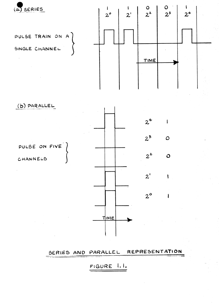
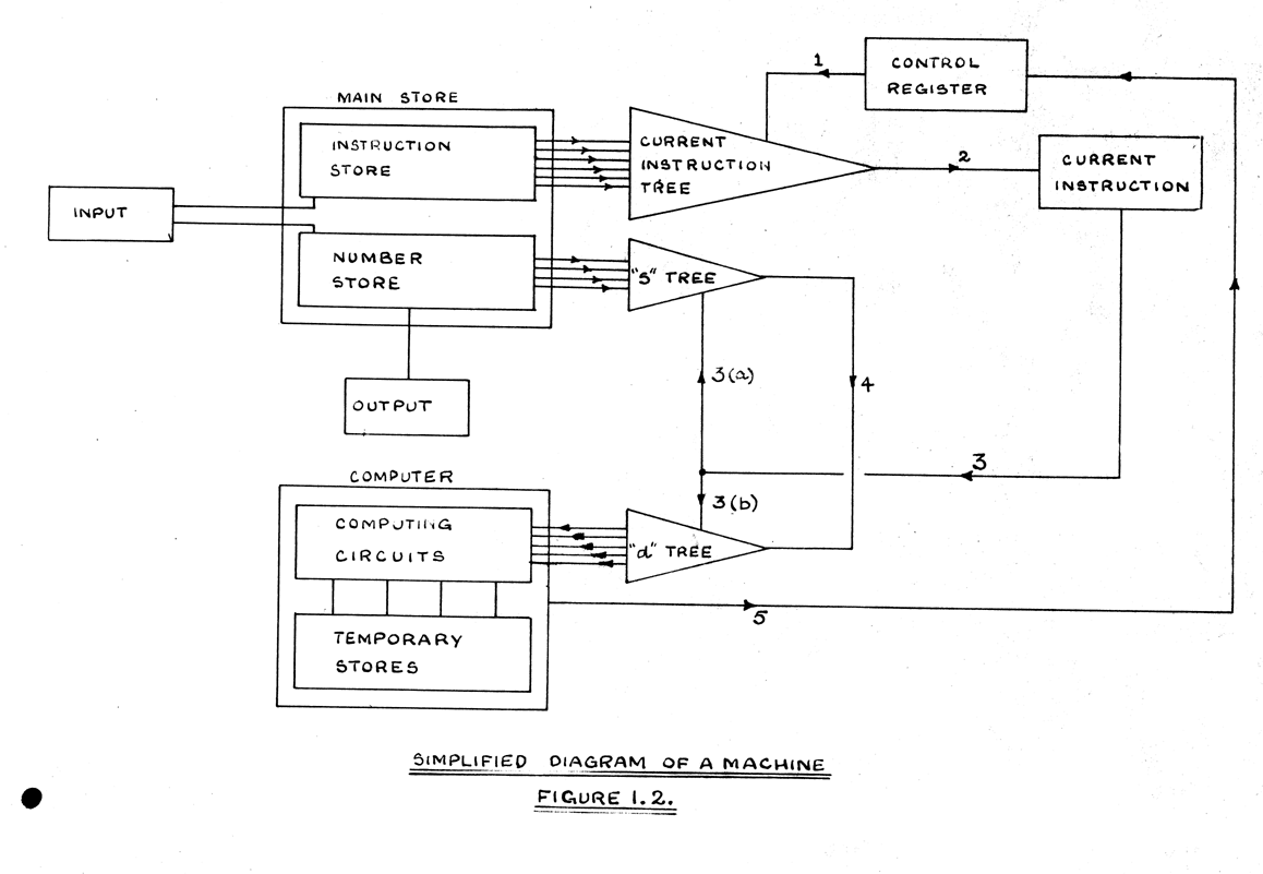
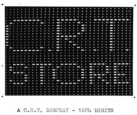
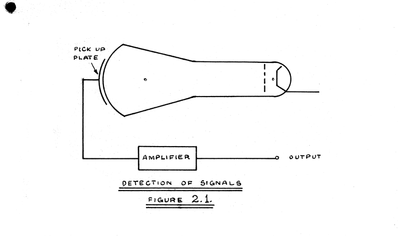
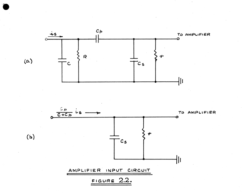
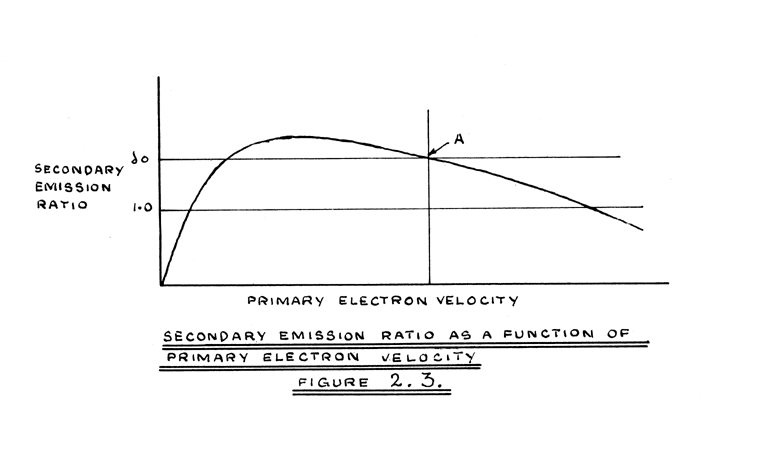
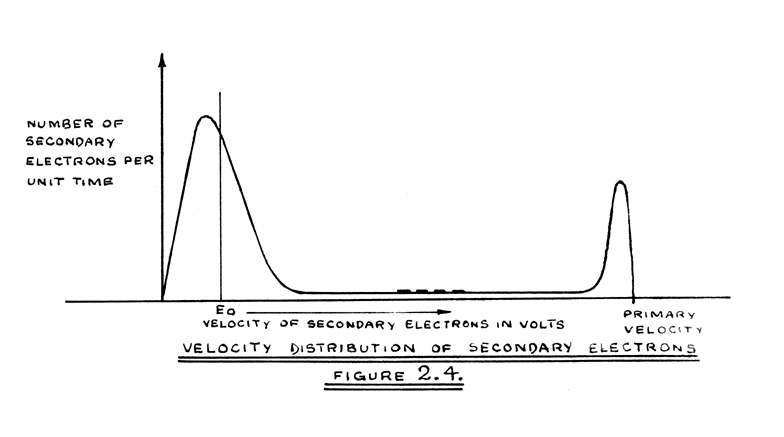
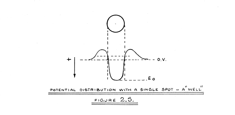
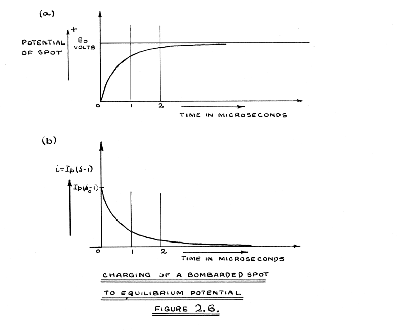
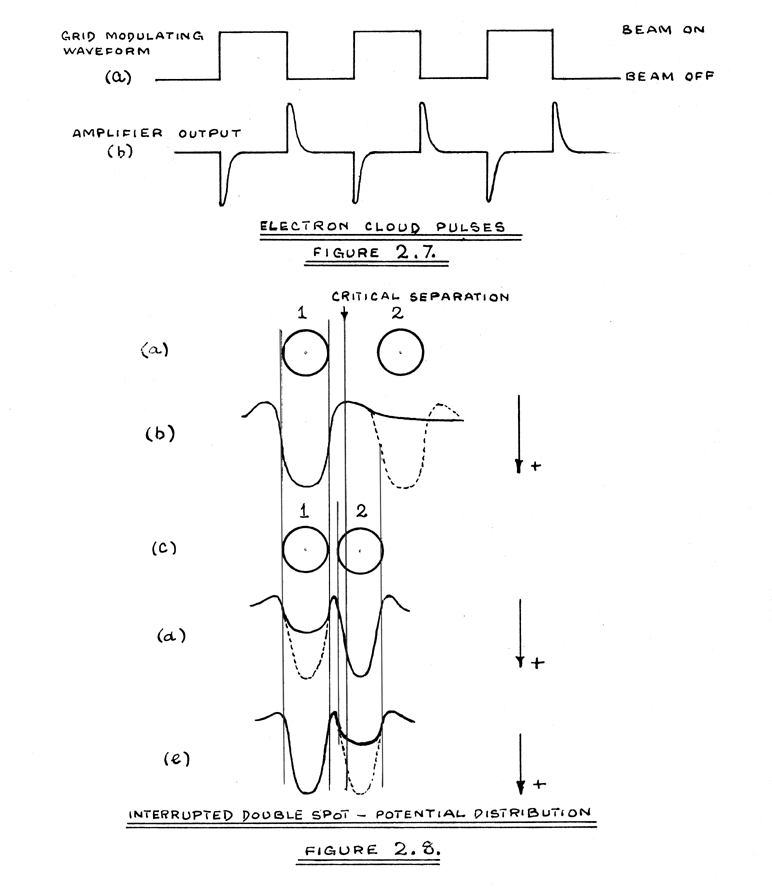
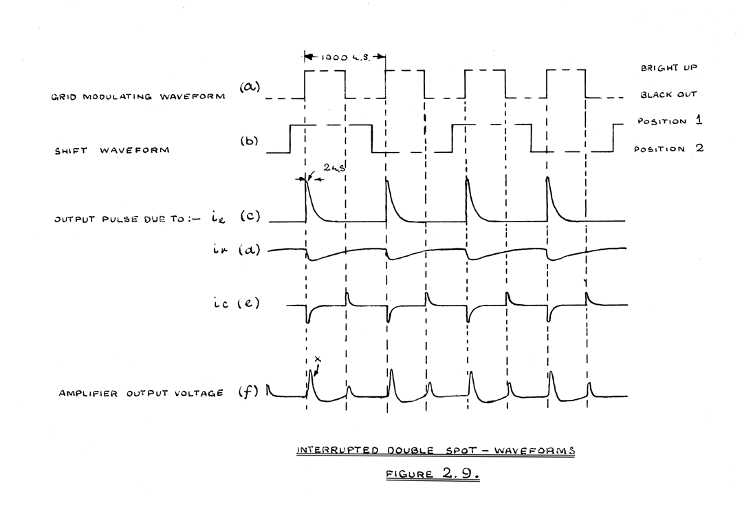
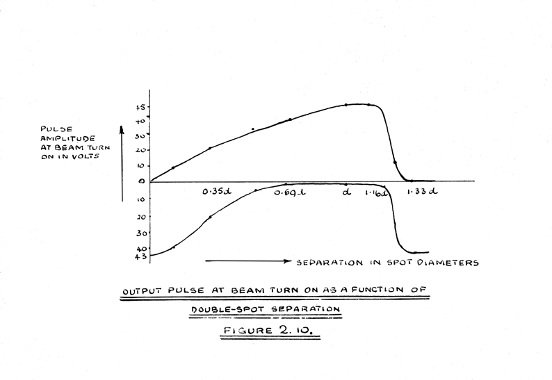
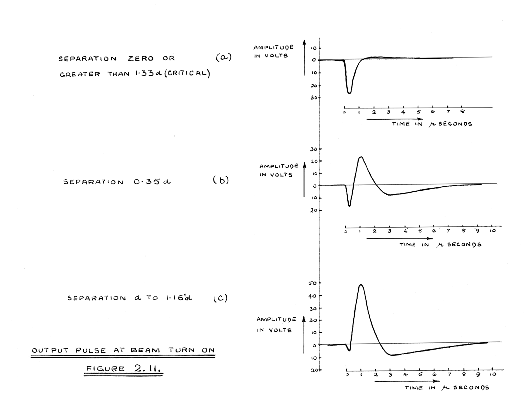
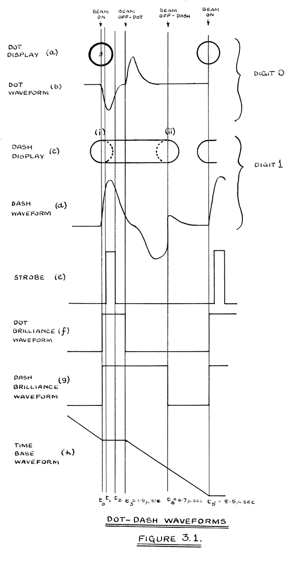
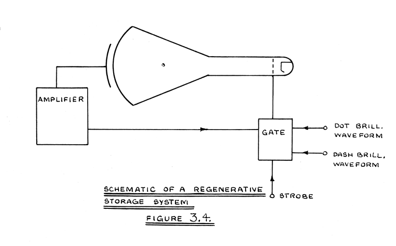
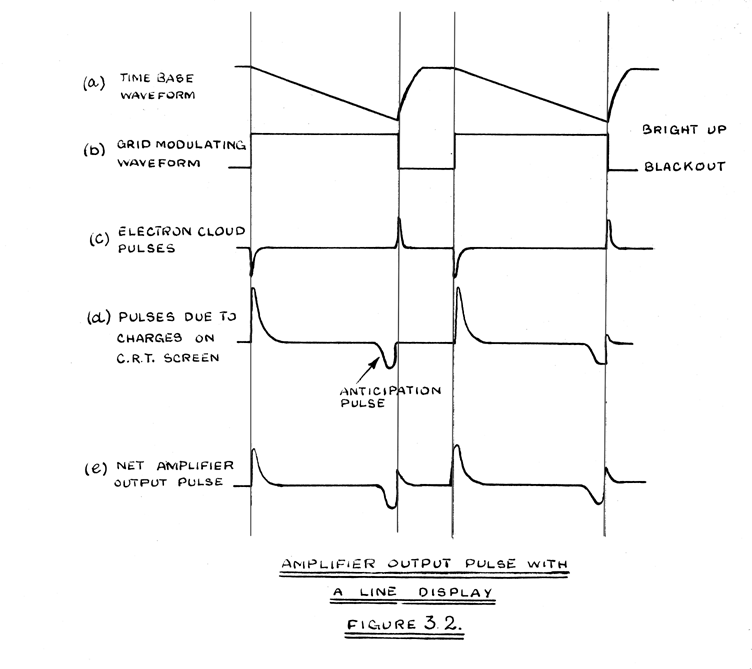
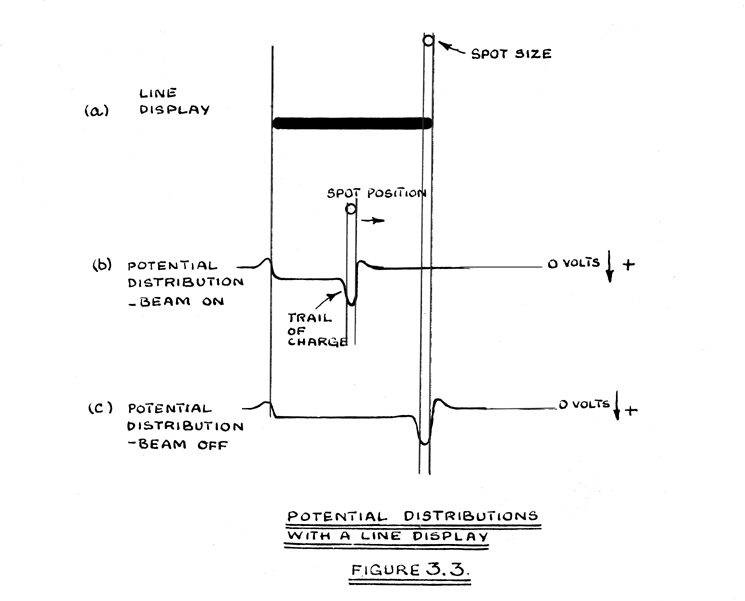
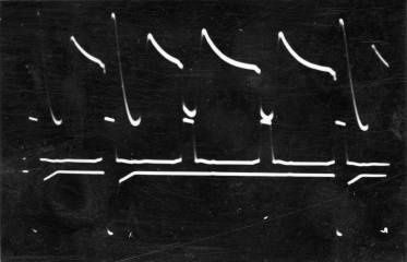
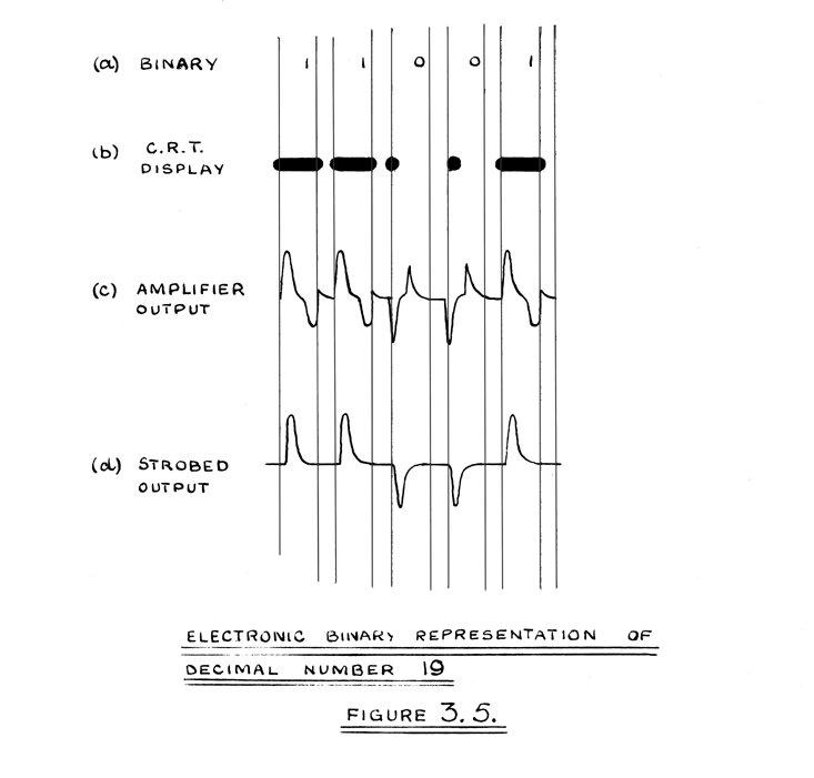
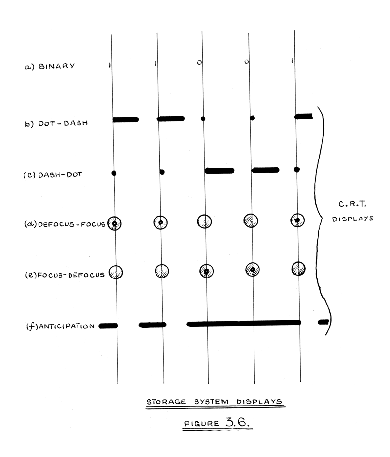
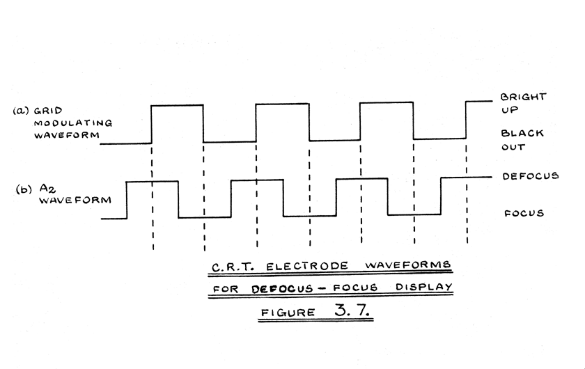
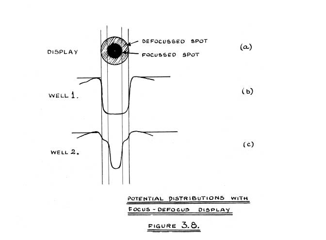
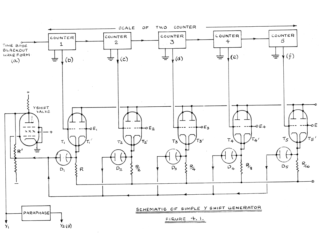
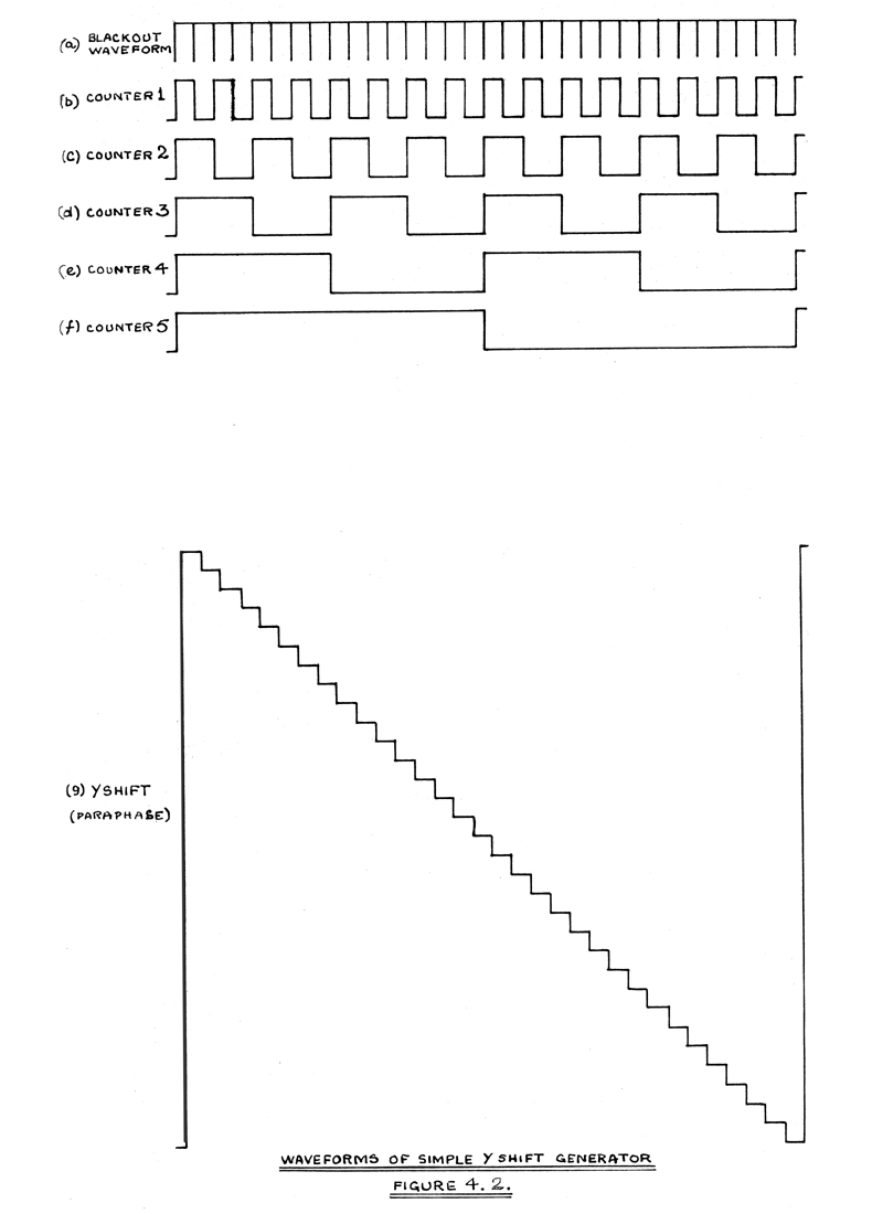
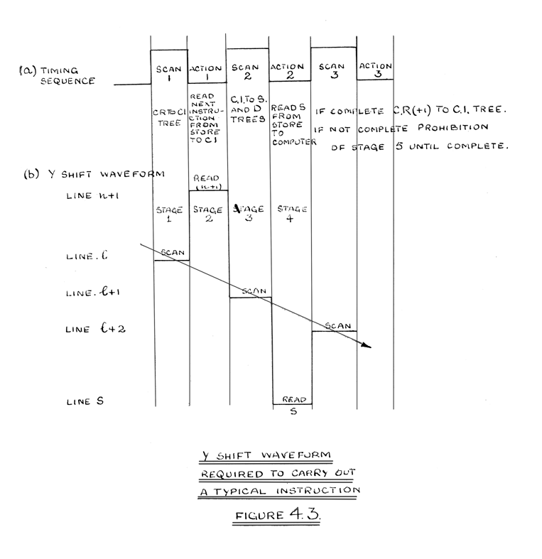
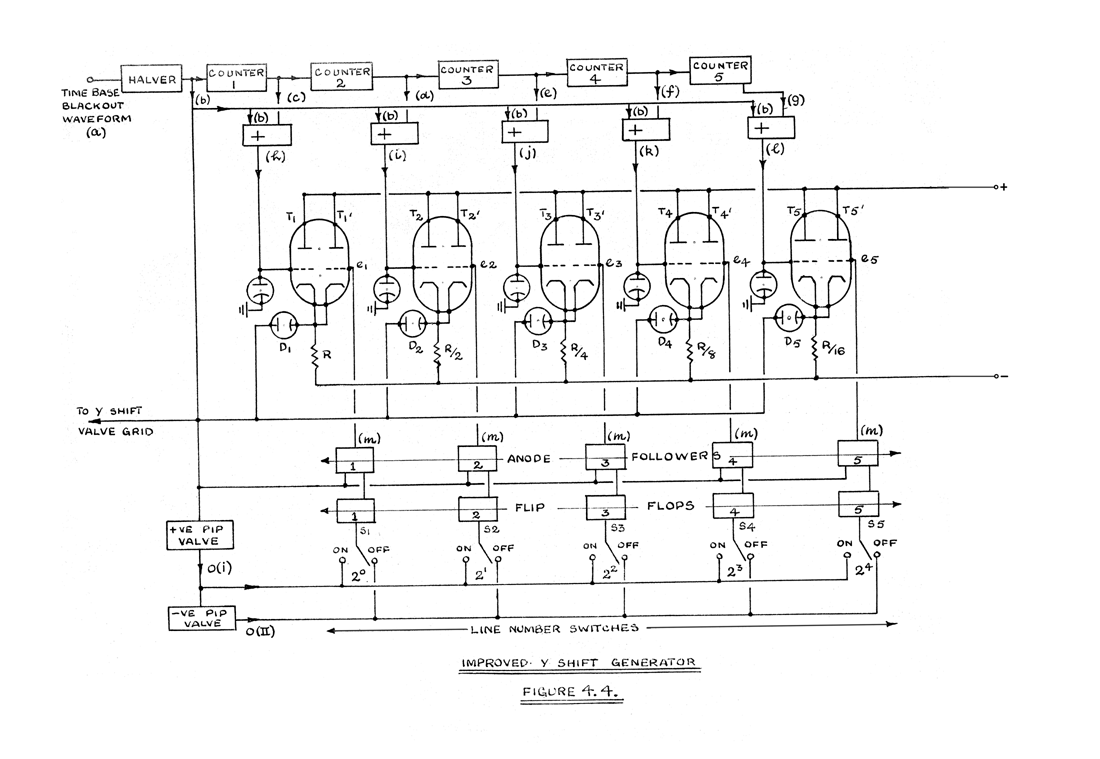
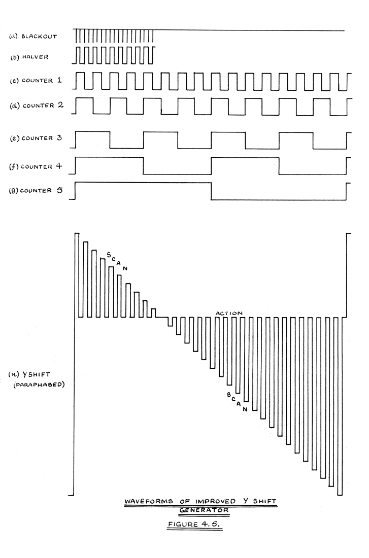
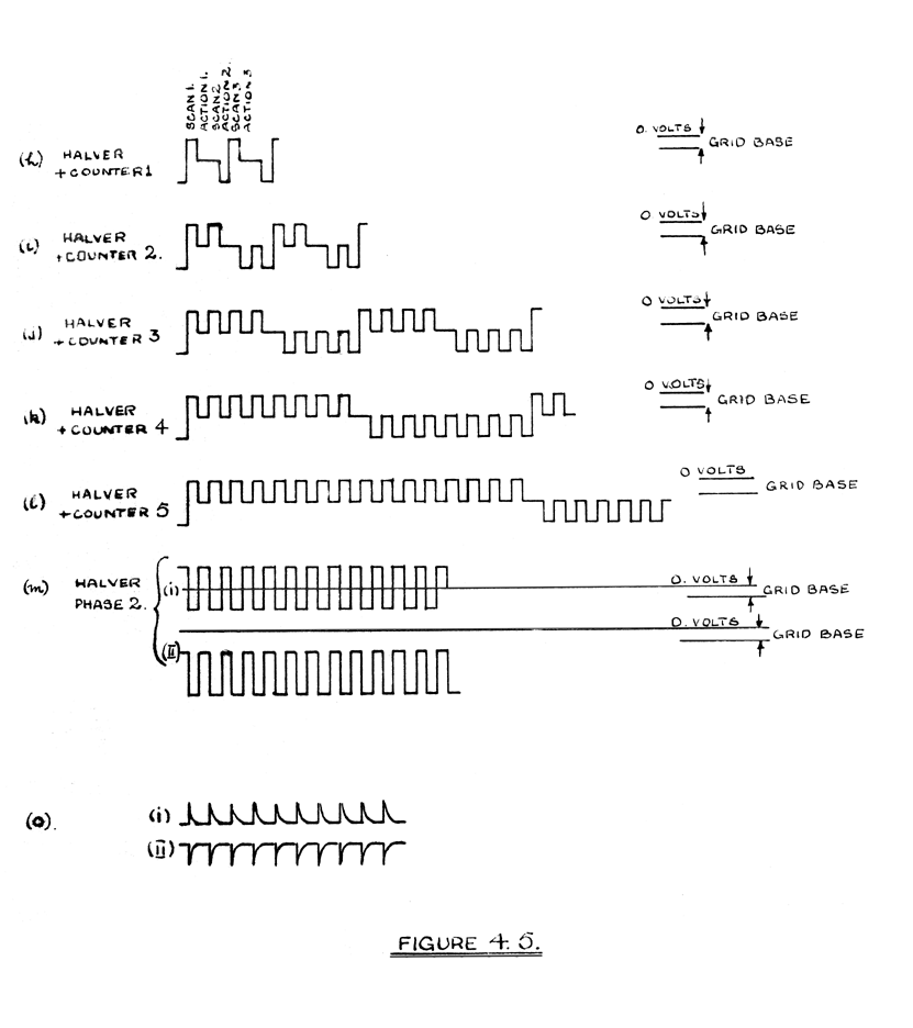
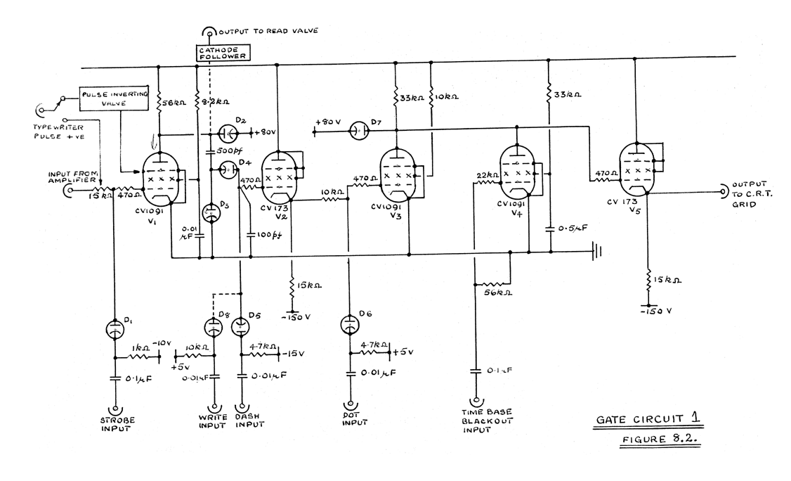
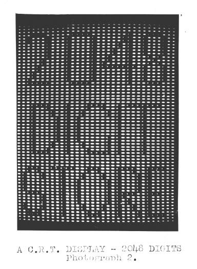
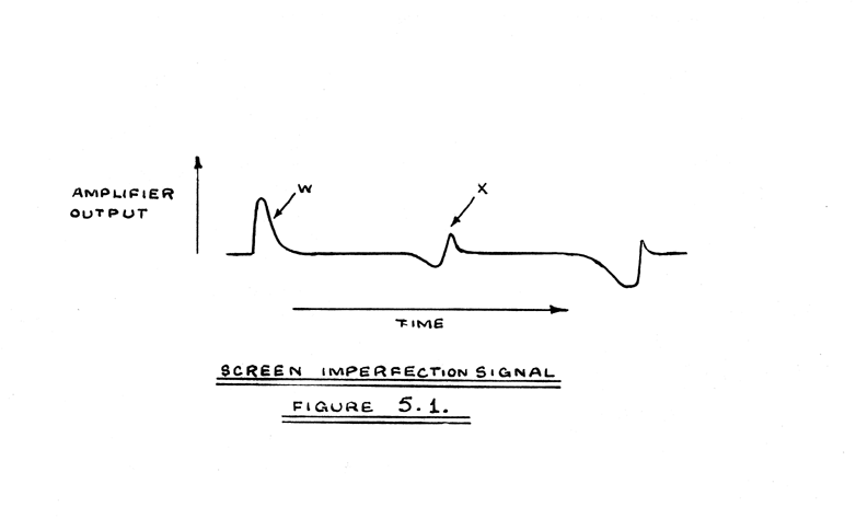
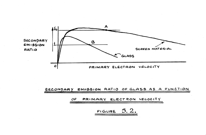
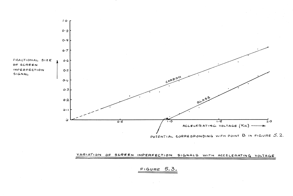
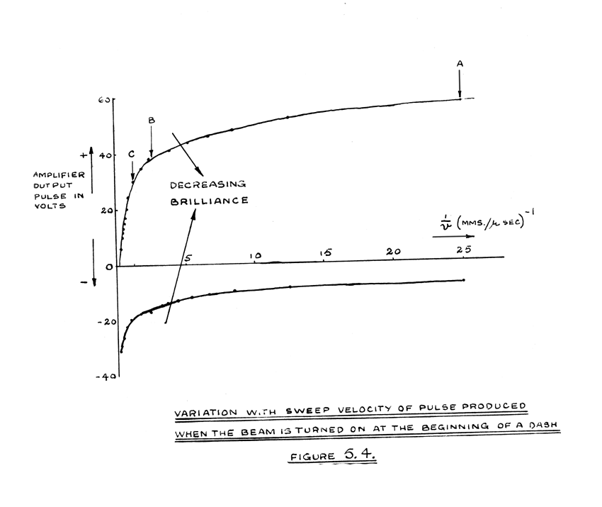
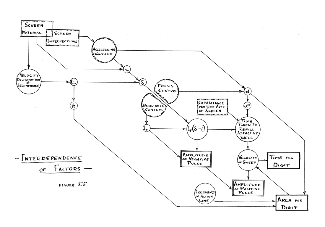
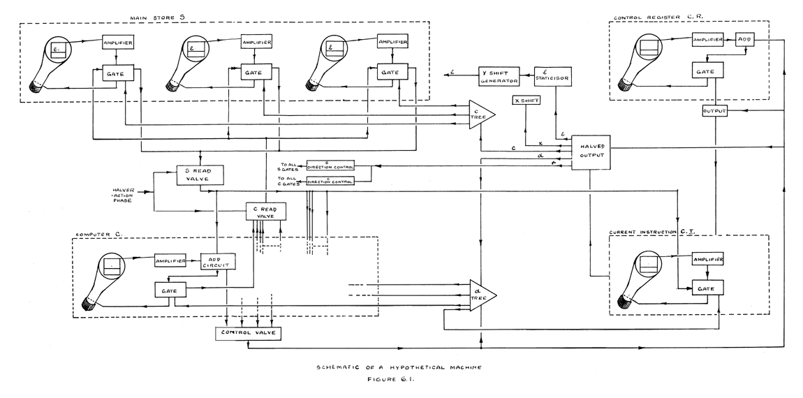
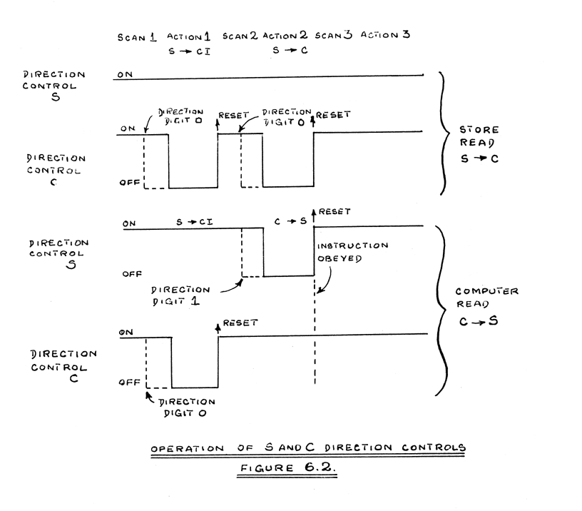
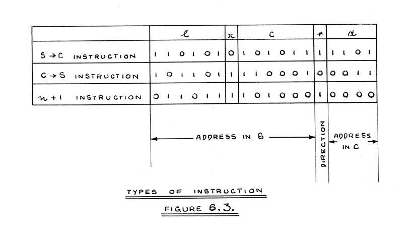
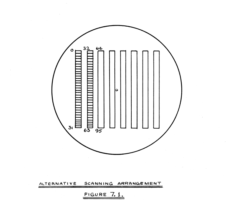
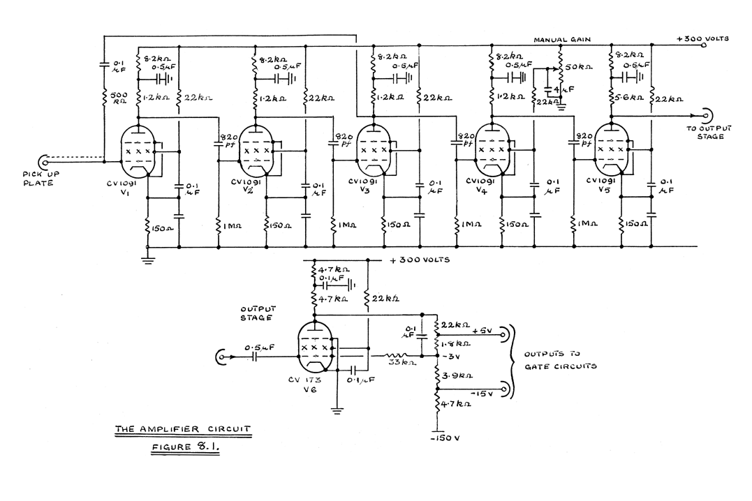
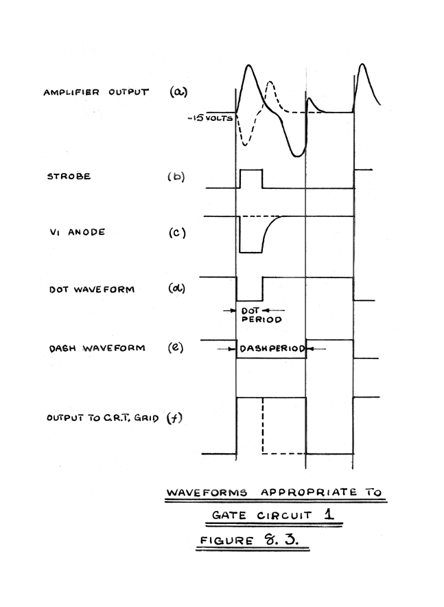
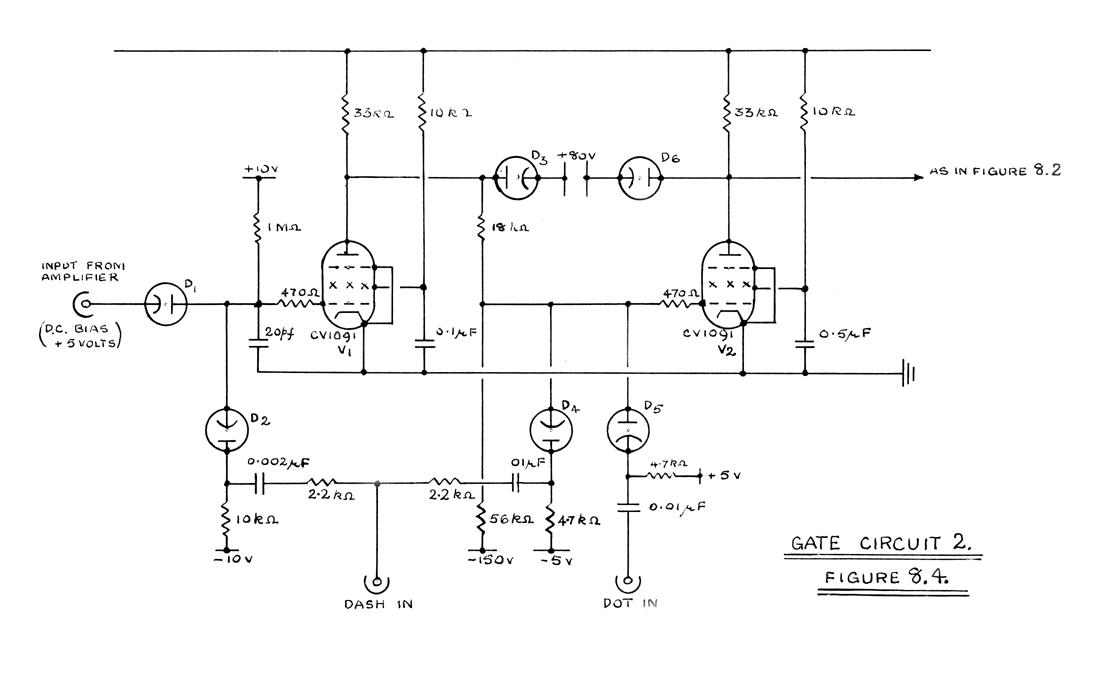
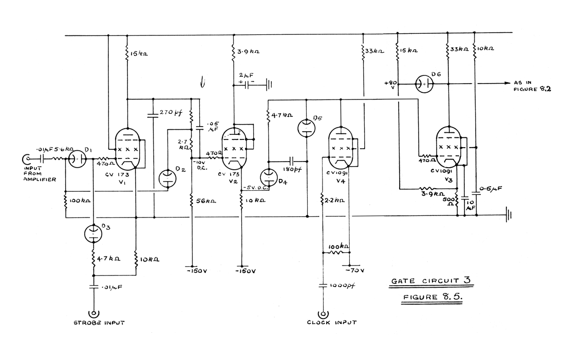
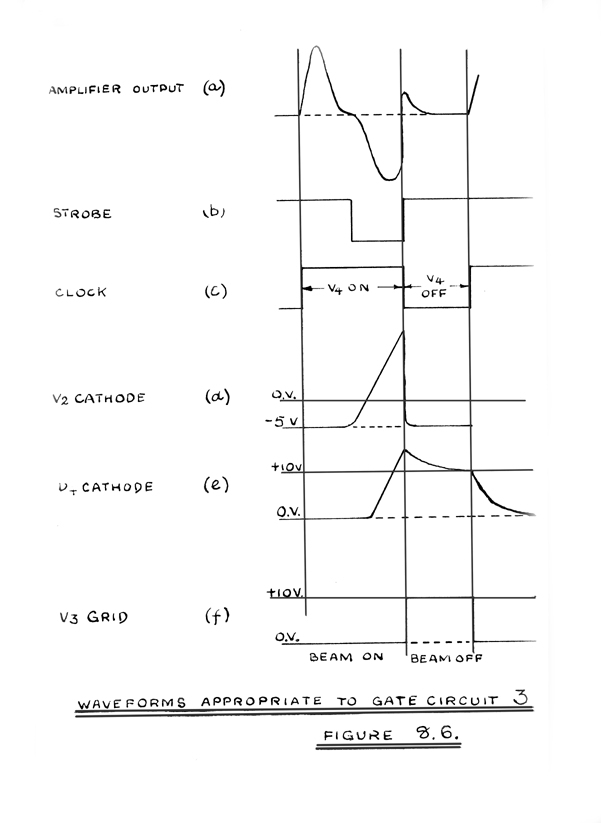